BULT118 STMicroelectronics, BULT118 Datasheet
BULT118
Specifications of BULT118
BULT118
Available stocks


Related parts for BULT118


BULT118 Summary of contents
Page 1
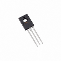
... RBSOA. The device is designed for use in lighting applications and low cost switch-mode power supplies. Table 1. Device summary Order code BULT118 July 2008 Figure 1. Marking Package BULT118 SOT-32 Rev 2 BULT118 SOT-32 Internal schematic diagram Packaging Tube www.st.com 1/10 10 ...
Page 2
... Emitter-base voltage (I EBO I Collector current C I Collector peak current ( Base current B I Base peak current ( Total dissipation at T tot T Storage temperature stg T Max. operating junction temperature J 2/10 Parameter = < 5 ms) P < °C c BULT118 Value Unit 700 V 400 -65 to 150 °C 150 °C ...
Page 3
... BULT118 2 Electrical characteristics (T = 25°C unless otherwise specified) case Table 3. Electrical characteristics Symbol Collector cut-off current I CES (V BE Collector-emitter leakage I CEO current V Emitter-base voltage EBO Collector-emitter (1) sustaining voltage V CEO(sus Collector-emitter (1) V CE(sat) saturation voltage Base-emitter saturation (1) V BE(sat) voltage ( current gain ...
Page 4
... Electrical characteristics 2.1 Electrical characteristics (curves) Figure 2. Safe operating area Figure 4. DC current gain Figure 6. Collector-emitter saturation voltage 4/10 Figure 3. Derating curve Figure 5. DC current gain Figure 7. Base-emitter saturation voltage BULT118 ...
Page 5
... BULT118 Figure 8. Inductive load fall time Figure 10. Resistive load fall time Figure 12. Reverse biased SOA Electrical characteristics Figure 9. Inductive load storage time Figure 11. Resistive load storage time 5/10 ...
Page 6
... Electrical characteristics 2.2 Test circuits Figure 13. Resistive load switching test circuit 1) Fast electronic switch 2) Non-inductive resistor Figure 14. Inductive load switching test circuit 1) Fast electronic switch 2) Non-inductive resistor 3) Fast recovery rectifier 6/10 BULT118 ...
Page 7
... BULT118 3 Package mechanical data In order to meet environmental requirements, ST offers these devices in ECOPACK® packages. These packages have a lead-free second level interconnect. The category of second level interconnect is marked on the package and on the inner box label, in compliance with JEDEC Standard JESD97. The maximum ratings related to soldering conditions are also marked on the inner box label ...
Page 8
... Package mechanical data DIM 8/10 SOT-32 (TO-126) MECHANICAL DATA mm. MIN. TYP 2.4 0.64 0.39 10.5 7.4 2.04 2.29 4.07 4.58 15.3 2.9 3.8 1 2.15 1.27 BULT118 MAX. 2.9 0.88 0.63 11.05 7.8 2.54 5.08 16 3.2 1.52 0016114E ...
Page 9
... BULT118 4 Revision history Table 4. Document revision history Date 29-Sep-2003 10-Jul-2008 Revision 1 Initial release. Updated: V condition in CEO(sus) 2 SOT-32 mechanical data, cover page Revision history Changes Table 3 on page 3, 9/10 ...
Page 10
... Australia - Belgium - Brazil - Canada - China - Czech Republic - Finland - France - Germany - Hong Kong - India - Israel - Italy - Japan - Malaysia - Malta - Morocco - Singapore - Spain - Sweden - Switzerland - United Kingdom - United States of America 10/10 Please Read Carefully: © 2008 STMicroelectronics - All rights reserved STMicroelectronics group of companies www.st.com BULT118 ...