NJW0281G ON Semiconductor, NJW0281G Datasheet

TRANS NPN BIPOLAR 15A TO-3P

NJW0281G

Manufacturer Part Number
NJW0281G
Description
TRANS NPN BIPOLAR 15A TO-3P
Manufacturer
ON Semiconductor
Datasheet

Specifications of NJW0281G

Transistor Type
NPN
Current - Collector (ic) (max)
15A
Voltage - Collector Emitter Breakdown (max)
250V
Vce Saturation (max) @ Ib, Ic
1V @ 500mA, 5A
Dc Current Gain (hfe) (min) @ Ic, Vce
75 @ 3A, 5V
Power - Max
150W
Frequency - Transition
30MHz
Mounting Type
Through Hole
Package / Case
TO-3P-3, TO-247-3
Transistor Polarity
NPN
Mounting Style
Through Hole
Collector- Emitter Voltage Vceo Max
250 V
Emitter- Base Voltage Vebo
5 V
Maximum Dc Collector Current
15 A
Power Dissipation
150000 mW
Maximum Operating Temperature
+ 150 C
Dc Collector/base Gain Hfe Min
75
Maximum Operating Frequency
30 MHz
Minimum Operating Temperature
- 65 C
Lead Free Status / RoHS Status
Lead free / RoHS Compliant
Current - Collector Cutoff (max)
-
Lead Free Status / Rohs Status
Lead free / RoHS Compliant

Available stocks

Company
Part Number
Manufacturer
Quantity
Price
Part Number:
NJW0281G
Manufacturer:
ON
Quantity:
14
Part Number:
NJW0281G
Manufacturer:
ONSEMICON
Quantity:
516
Part Number:
NJW0281G
Manufacturer:
ON/安森美
Quantity:
20 000
Company:
Part Number:
NJW0281G
Quantity:
18 000
Part Number:
NJW0281G/NJW0302G
Manufacturer:
MICRON
Quantity:
1 000
NJW0281G (NPN)
NJW0302G (PNP)
Complementary NPN-PNP
Power Bipolar Transistors
popular NJW3281G and NJW1302G audio output transistors. With
superior gain linearity and safe operating area performance, these
transistors are ideal for high fidelity audio amplifier output stages and
other linear applications.
Features
Benefits
Applications
Stresses exceeding Maximum Ratings may damage the device. Maximum
Ratings are stress ratings only. Functional operation above the Recommended
Operating Conditions is not implied. Extended exposure to stresses above the
Recommended Operating Conditions may affect device reliability.
1. Pulse Test: Pulse Width = 5.0 ms, Duty Cycle < 10%.
© Semiconductor Components Industries, LLC, 2008
January, 2008 - Rev. 0
MAXIMUM RATINGS
Collector-Emitter Voltage
Collector-Base Voltage
Emitter-Base Voltage
Collector-Emitter Voltage - 1.5 V
Collector Current - Continuous
Collector Current
Base Current - Continuous
Total Power Dissipation @ T
Operating and Storage Junction
These complementary devices are lower power versions of the
Exceptional Safe Operating Area
NPN/PNP Gain Matching within 10% from 50 mA to 3 A
Excellent Gain Linearity
High BVCEO
High Frequency
These are Pb-Free Devices
Reliable Performance at Higher Powers
Symmetrical Characteristics in Complementary Configurations
Accurate Reproduction of Input Signal
Greater Dynamic Range
High Amplifier Bandwith
High-End Consumer Audio Products
Professional Audio Amplifiers
Temperature Range
Home Amplifiers
Home Receivers
Theater and Stadium Sound Systems
Public Address Systems (PAs)
Rating
- Peak (Note 1)
Preferred Devices
C
= 25°C
Symbol
T
V
V
V
V
J
P
CEO
CBO
EBO
, T
CEX
I
I
C
B
D
stg
- 65 to
Value
+150
250
250
250
150
5.0
1.5
15
30
1
Watts
Unit
Vdc
Vdc
Vdc
Vdc
Adc
Adc
°C
Preferred devices are recommended choices for future use
and best overall value.
NJW0281G
NJW0302G
COMPLEMENTARY SILICON
Device
POWER TRANSISTORS
250 VOLTS, 150 WATTS
ORDERING INFORMATION
xxxx
G
A
Y
WW
http://onsemi.com
15 AMPERES
CASE 340AB
(Pb-Free)
(Pb-Free)
Package
= 0281 or 0302
= Pb-Free Package
= Assembly Location
= Year
= Work Week
TO-3P
TO-3P
TO-3P
Publication Order Number:
30 Units/Rail
30 Units/Rail
MARKING
DIAGRAM
NJWxxxG
Shipping
AYWW
NJW0281/D

Related parts for NJW0281G

NJW0281G Summary of contents

Page 1

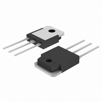
... NJW0281G (NPN) NJW0302G (PNP) Preferred Devices Complementary NPN-PNP Power Bipolar Transistors These complementary devices are lower power versions of the popular NJW3281G and NJW1302G audio output transistors. With superior gain linearity and safe operating area performance, these transistors are ideal for high fidelity audio amplifier output stages and other linear applications ...

Page 2

... Output Capacitance ( 1.0 MHz test 160 140 120 100 100 T , CASE TEMPERATURE (°C) C Figure 1. Power Derating NJW0281G (NPN) NJW0302G (PNP 25°C unless otherwise noted) C 100 10 1 0.1 0.01 1 120 140 160 http://onsemi.com 2 Symbol Value R 0.83 θJC Symbol Min Max V 250 - CEO(sus) ...

Page 3

... NJW0281G (NPN) NJW0302G (PNP) 500 100°C 100 -25°C 25°C 10 0.05 0 COLLECTOR CURRENT (A) C Figure 3. NJW0281G DC Current Gain 1 5 1.2 1 -25°C 0.8 0.6 25°C 100°C 0.4 0.2 0 0.01 0 COLLECTOR CURRENT (A) C Figure 5. NJW0281G Base-Emitter Voltage 100°C 25°C 0.1 -25° ...

Page 4

... NJW0281G (NPN) NJW0302G (PNP 5 25° 0.01 0 COLLECTOR CURRENT (A) C Figure 9. NJW0281G Current Gain Bandwidth Product 5 25° 0.01 Figure 10. NJW0302G Current Gain Bandwidth http://onsemi.com 4 0 COLLECTOR CURRENT (A) C Product 10 ...

Page 5

... LITERATURE FULFILLMENT:  Literature Distribution Center for ON Semiconductor   Box 5163, Denver, Colorado 80217 USA   Phone: 303-675-2175 or 800-344-3860 Toll Free USA/Canada   Fax: 303-675-2176 or 800-344-3867 Toll Free USA/Canada   Email: orderlit@onsemi.com NJW0281G (NPN) NJW0302G (PNP) PACKAGE DIMENSIONS TO-3P-3LD CASE 340AB-01 ISSUE A SEATING ...

Related keywords