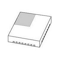
TDA8263HN/C1-T NXP Semiconductors, TDA8263HN/C1-T Datasheet - Page 21

TDA8263HN/C1-T
Manufacturer Part Number
TDA8263HN/C1-T
Description
Tuners INTEGRATED SATELLITE TUNER
Manufacturer
NXP Semiconductors
Datasheet
1.TDA8263HNC1-T.pdf
(28 pages)
Specifications of TDA8263HN/C1-T
Bus Type
I2C
Maximum Agc
60 dB
Maximum Frequency
2175 MHz
Minimum Frequency
950 MHz
Modulation Technique
QPSK
Mounting Style
SMD/SMT
Package / Case
HVQFN-32
Function
Satellite
Noise Figure
7.7 dB
Operating Supply Voltage
3.3 V
Supply Voltage (min)
3.15 V
Supply Voltage (max)
3.45 V
Minimum Operating Temperature
- 20 C
Maximum Operating Temperature
+ 85 C
Lead Free Status / RoHS Status
Lead free / RoHS Compliant
Other names
TDA8263HN/C1,518
Philips Semiconductors
Table 39:
T
[1]
[2]
9397 750 13193
Product data sheet
Symbol
SNF
MDR
Crystal oscillator and XTOUT
Z
f
Z
V
MS input
I
I
Charge pump and tuning voltage
I
I
I
I
I
I
SDA and SCL input
V
V
I
I
f
SDA output
V
AS input
I
I
PORTn
V
XTAL
h
l
l
l(min)
l(max)
h(min)
h(max)
2
HI
LI
SCL
ASh
ASl
amb
osc
XTAL
o(p-p)
C-bus and PORTn
IL
IH
O
O(max)
N
osc
The product is qualified with an output voltage of 550 mV (p-p) differential, however larger values can be used at baseband outputs that
might have impact on the product performance.
IIP
Wanted signal: RF1 is 2140 MHz, P
is P1.
SB
= 25 C; V
2
= 20 + (P1
Characteristics
Parameter
oscillator phase noise in the
satellite band
synthesizer noise floor in the
satellite band
main divider ratio
crystal oscillator negative
impedance
crystal frequency
recommended crystal series
resistance
output voltage (peak-to-peak value) crystal output
HIGH level input current
LOW level input current
charge pump leakage current
charge pump low, minimum current CPHIGH = 0 and CPCURSEL = 0
charge pump low, maximum
current
charge pump high, minimum
current
charge pump high, maximum
current
LOW-level input voltage
HIGH-level input voltage
HIGH-level leakage current
LOW-level leakage current
input clock frequency
output voltage during acknowledge I
high level input current
low level input current
PORTn maximum output voltage
CC
= 3.3 V; output level on differential I/Q output is 550 mV (p-p); unless otherwise specified.
P2) [dBm].
…continued
RFIN
= 20 dBm and the AGC adjusted to get 550 mV (p-p) on the differential output. The output level
Rev. 01 — 14 December 2004
Conditions
100 kHz offset, out of the PLL
bandwidth
1 kHz and 10 kHz offset;
f
absolute value
V
V
CPHIGH = 0 and CPCURSEL = 1
CPHIGH = 1 and CPCURSEL = 0
CPHIGH = 1 and CPCURSEL = 1
5 V and 3.3 V bus
5 V and 3.3 V bus
V
V
V
V
I
comp
sink
sink
MS
MS
IH
IL
AS
AS
= 0 V; V
= 3.3 V; V
= 3 mA
= 9 mA
= V
= 0 V
= V
= 0 V
= 1 MHz
CC
CC
CC
CC
= 3.3 V
= 0 V or 3.3 V
[4]
[4]
Fully integrated satellite tuner
© Koninklijke Philips Electronics N.V. 2004. All rights reserved.
Min
-
-
128
500
16
-
550
0.67
0.97
1.27
1.87
-
2.3
-
-
-
-
50
50
10
10
100
100
TDA8263HN
Typ
-
-
-
16
-
750
-
-
0
0.9
1.3
1.7
2.5
-
-
-
-
-
-
-
-
-
100
Max
32767
-
16
150
-
+50
+50
+10
1.13
1.63
2.13
3.13
0.99
-
10
-
400
0.4
+100
+100
0.4
94
78
Unit
dBc/Hz
dBc/Hz
MHz
mV
nA
mA
mA
mA
mA
V
V
kHz
V
V
A
A
A
A
A
A
21 of 28


