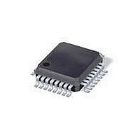
PCK953BD NXP Semiconductors, PCK953BD Datasheet - Page 6

PCK953BD
Manufacturer Part Number
PCK953BD
Description
Phase Locked Loops (PLL) 50-125MHZPECL IP/1.8SDRAM CKDR
Manufacturer
NXP Semiconductors
Type
PLL Clock Driverr
Datasheet
1.PCK953BDG128.pdf
(15 pages)
Specifications of PCK953BD
Number Of Circuits
1
Maximum Input Frequency
125 MHz
Minimum Input Frequency
20 MHz
Output Frequency Range
35 MHz to 125 MHz
Supply Voltage (max)
3.465 V
Supply Voltage (min)
3.135 V
Maximum Operating Temperature
+ 70 C
Minimum Operating Temperature
0 C
Mounting Style
SMD/SMT
Operating Supply Voltage
3.3 V
Package / Case
LQFP-32
Lead Free Status / RoHS Status
Lead free / RoHS Compliant
Other names
PCK953BD,157
Available stocks
Company
Part Number
Manufacturer
Quantity
Price
Company:
Part Number:
PCK953BD
Manufacturer:
PHILIPS
Quantity:
2 295
Part Number:
PCK953BD
Manufacturer:
PHILIPS/飞利浦
Quantity:
20 000
Company:
Part Number:
PCK953BD,118
Manufacturer:
NXP Semiconductors
Quantity:
10 000
Company:
Part Number:
PCK953BD,128
Manufacturer:
NXP Semiconductors
Quantity:
10 000
Company:
Part Number:
PCK953BD,157
Manufacturer:
NXP Semiconductors
Quantity:
10 000
Part Number:
PCK953BD/G
Manufacturer:
NXP/恩智浦
Quantity:
20 000
Company:
Part Number:
PCK953BD/G,128
Manufacturer:
NXP Semiconductors
Quantity:
10 000
Company:
Part Number:
PCK953BD/G128
Manufacturer:
NXP Semiconductors
Quantity:
135
NXP Semiconductors
11. Application information
PCK953_5
Product data sheet
11.1 Power supply filtering
The PCK953 is a mixed analog/digital product and as such it exhibits some sensitivities
that would not necessarily be seen on a fully digital product. Analog circuitry is naturally
susceptible to random noise, especially if this noise is seen on the power supply pins. The
PCK953 provides separate power supplies for the output buffers (V
phase-locked loop (V
isolate the high switching noise digital outputs from the relatively sensitive internal analog
phase-locked loop. In a controlled environment such as an evaluation board, this level of
isolation is sufficient. However, in a digital system environment where it is more difficult to
minimize noise on the power supplies, a second level of isolation may be required. The
simplest form of isolation is a power supply filter on the V
Figure 3
to noise with spectral content in the 1 kHz to 1 MHz range. Therefore, the filter should be
designed to target this range. The key parameter that needs to be met in the final filter
design is the DC voltage drop that will be seen between the V
of the PCK953. The current sourced though the V
maximum), assuming that a minimum of 3.0 V must be maintained on the V
very little DC voltage drop can be tolerated when a 3.3 V V
shown in
criteria. The RC filter pictured will provide a broadband filter with approximately 100 : 1
attenuation for noise whose spectral content is above 20 kHz. As the noise frequency
crosses the series resonant point of an individual capacitor, its overall impedance begins
to look inductive, and thus increases with increasing frequency. The parallel capacitor
combination shown ensures that a low impedance path to ground exists for frequencies
well above the bandwidth of the PLL. It is recommended that the user start with an 8
10
resistors when a higher level of attenuation is shown to be needed.
Although the PCK953 has several design features to minimize the susceptibility to power
supply noise (isolated power and grounds and fully differential PLL) there still may be
applications in which overall performance is being degraded due to system power supply
noise. The power supply filter schemes discussed in this section should be adequate to
eliminate power supply noise related problems in most designs.
Fig 3.
resistor to avoid potential V
illustrates a typical power supply filter scheme. The PCK953 is most susceptible
Figure 3
Power supply filter
20 MHz to 125 MHz PECL input, 9 CMOS output, 3.3 V PLL clock driver
must have a resistance of 10
CCA
Rev. 05 — 9 October 2008
) of the device. The purpose of this design technique is to try to
PCK953
CC
V
drop problems, and only move to the higher value
V
CCA
CC
0.01 F
R s = 5
CCA
to 15
to 15
22 F
pin is typically 15 mA (20 mA
0.01 F
3.3 V
002aae139
CCA
to meet the voltage drop
CC
pin for the PCK953.
supply is used. The resistor
CC
supply and the V
CCO
) and the
© NXP B.V. 2008. All rights reserved.
PCK953
CCA
pin,
CCA
6 of 15
pin
to


