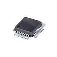
PCK953BD NXP Semiconductors, PCK953BD Datasheet - Page 4

PCK953BD
Manufacturer Part Number
PCK953BD
Description
Phase Locked Loops (PLL) 50-125MHZPECL IP/1.8SDRAM CKDR
Manufacturer
NXP Semiconductors
Type
PLL Clock Driverr
Datasheet
1.PCK953BDG128.pdf
(15 pages)
Specifications of PCK953BD
Number Of Circuits
1
Maximum Input Frequency
125 MHz
Minimum Input Frequency
20 MHz
Output Frequency Range
35 MHz to 125 MHz
Supply Voltage (max)
3.465 V
Supply Voltage (min)
3.135 V
Maximum Operating Temperature
+ 70 C
Minimum Operating Temperature
0 C
Mounting Style
SMD/SMT
Operating Supply Voltage
3.3 V
Package / Case
LQFP-32
Lead Free Status / RoHS Status
Lead free / RoHS Compliant
Other names
PCK953BD,157
Available stocks
Company
Part Number
Manufacturer
Quantity
Price
Company:
Part Number:
PCK953BD
Manufacturer:
PHILIPS
Quantity:
2 295
Part Number:
PCK953BD
Manufacturer:
PHILIPS/飞利浦
Quantity:
20 000
Company:
Part Number:
PCK953BD,118
Manufacturer:
NXP Semiconductors
Quantity:
10 000
Company:
Part Number:
PCK953BD,128
Manufacturer:
NXP Semiconductors
Quantity:
10 000
Company:
Part Number:
PCK953BD,157
Manufacturer:
NXP Semiconductors
Quantity:
10 000
Part Number:
PCK953BD/G
Manufacturer:
NXP/恩智浦
Quantity:
20 000
Company:
Part Number:
PCK953BD/G,128
Manufacturer:
NXP Semiconductors
Quantity:
10 000
Company:
Part Number:
PCK953BD/G128
Manufacturer:
NXP Semiconductors
Quantity:
135
NXP Semiconductors
7. Limiting values
8. Static characteristics
Table 5.
T
[1]
[2]
PCK953_5
Product data sheet
Symbol
V
V
V
V
V
V
I
C
C
I
I
I
CC
CCPLL
amb
IH
IL
i(p-p)
cm
OH
OL
i
PD
V
within the V
The PCK953 outputs can drive series or parallel terminated 50
Section 11 “Application
= 0 C to 70 C; V
cm
is the difference from the most positive side of the differential input signal. Normal operation is obtained when the HIGH input is
Static characteristics
Parameter
HIGH-level input voltage
LOW-level input voltage
peak-to-peak input voltage
common-mode voltage
HIGH-level output voltage
LOW-level output voltage
input current
input capacitance
power dissipation capacitance
maximum quiescent supply current
maximum PLL supply current
cm
range and the input swing lies within the V
CC
Table 4.
In accordance with the Absolute Maximum Rating System (IEC 60134).
Symbol
V
V
I
T
information”).
I
= 3.3 V
stg
CC
I
5 %, unless specified otherwise.
Limiting values
Parameter
supply voltage
input voltage
input current
storage temperature
20 MHz to 125 MHz PECL input, 9 CMOS output, 3.3 V PLL clock driver
Rev. 05 — 9 October 2008
Conditions
LVCMOS inputs
LVCMOS inputs
PECL_CLK
PECL_CLK
I
I
per output
all V
V
OH
OL
CCA
= 20 mA
= 20 mA
i(p-p)
CC
pin only
pins
specification.
(or 50
Conditions
to 0.5V
[1]
[2]
[2]
CC
Min
2.0
-
300
V
2.4
-
-
-
-
-
-
) transmission lines on the incident edge (see
CC
1.5
Min
-
Typ
-
-
-
-
-
-
-
-
25
9
9
0.3
0.3
40
Max
+4.6
V
+125
20
Max
3.6
0.8
1000
V
-
0.5
4
-
20
20
© NXP B.V. 2008. All rights reserved.
DD
75
CC
PCK953
+ 0.3
0.6
Unit
V
V
mA
Unit
V
V
mV
mV
V
V
pF
pF
mA
mA
C
A
4 of 15


