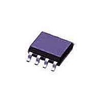
TJA1020TD NXP Semiconductors, TJA1020TD Datasheet - Page 3

TJA1020TD
Manufacturer Part Number
TJA1020TD
Description
RF Transceiver LIN TRANSCEIVER
Manufacturer
NXP Semiconductors
Datasheet
1.TJA1020TD.pdf
(22 pages)
Specifications of TJA1020TD
Number Of Receivers
4
Number Of Transmitters
3
Operating Supply Voltage
5 V to 27 V
Maximum Operating Temperature
+ 150 C
Mounting Style
SMD/SMT
Package / Case
SO-8
Maximum Data Rate
0.02 MBd
Maximum Supply Current
8 mA
Minimum Operating Temperature
- 40 C
Lead Free Status / RoHS Status
Lead free / RoHS Compliant
Other names
TJA1020T/N1,112
Philips Semiconductors
BLOCK DIAGRAM
PINNING
2004 Jan 13
handbook, full pagewidth
RXD
NSLP
NWAKE
TXD
GND
LIN
BAT
INH
SYMBOL
LIN transceiver
NWAKE
NSLP
RXD
TXD
PIN
BAT
1
2
3
4
5
6
7
8
receive data output (open-drain);
active LOW after a wake-up event
sleep control input (active LOW);
controls inhibit output; resets
wake-up source flag on TXD and
wake-up request on RXD
local wake-up input (active LOW);
negative edge triggered
transmit data input; active LOW
output after a local wake-up event
ground
LIN bus line input/output
battery supply
battery related inhibit output for con-
trolling an external voltage regulator;
active HIGH after a wake-up event
2
4
1
7
3
DESCRIPTION
TIME-OUT
NORMAL
WAKE-UP
SLEEP/
TIMER
TIMER
TIMER
TXD
RXD/
INT
Fig.1 Block diagram.
TJA1020T
TEMPERATURE
PROTECTION
3
CONTROL
TIMER
BUS
handbook, halfpage
NWAKE
NSLP
RXD
TXD
Fig.2 Pinning diagram.
1
2
3
4
FILTER
TJA1020T
MGU242
MGU241
8
7
6
5
Product specification
8
6
5
INH
BAT
LIN
GND
TJA1020
INH
LIN
GND


