MJ11022G ON Semiconductor, MJ11022G Datasheet - Page 3
MJ11022G
Manufacturer Part Number
MJ11022G
Description
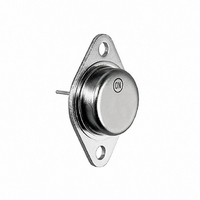
TRANS DARL NPN 15A 250V TO-3
Manufacturer
ON Semiconductor
Datasheet
1.MJ11021G.pdf
(5 pages)
Specifications of MJ11022G
Transistor Type
NPN - Darlington
Current - Collector (ic) (max)
15A
Voltage - Collector Emitter Breakdown (max)
250V
Vce Saturation (max) @ Ib, Ic
3.4V @ 150mA, 15A
Current - Collector Cutoff (max)
1mA
Dc Current Gain (hfe) (min) @ Ic, Vce
400 @ 10A, 5V
Power - Max
175W
Mounting Type
Chassis Mount
Package / Case
TO-204, TO-3
Lead Free Status / RoHS Status
Lead free / RoHS Compliant
Frequency - Transition
-
Other names
MJ11022G
MJ11022GOS
MJ11022GOS


FORWARD BIAS
a transistor average junction temperature and second
breakdown. Safe operating area curves indicate I
limits of the transistor that must be observed for reliable
operation, i.e., the transistor must not be subjected to greater
dissipation than the curves indicate.
variable dependIng on conditions. Second breakdown pulse
limits are valid for duty cycles to 10% provided T
v 175_C. T
Figure 3. At high case temperatures thermal limitations will
reduce the power that can be handled to values less than the
limitations imposed by second breakdown.
There are two limitations on the power handling ability of
The data of Figure 4 is based on T
5.0
3.0
2.0
1.0
0.5
0.3
0.2
30
20
10
0
3.0
0.07
0.05
0.03
0.02
0.01
1.0
0.7
0.5
0.3
0.2
0.1
Figure 4. Maximum Rated Forward Bias Safe
0.01
5.0
SINGLE PULSE
D = 0.5
J(pk)
V
0.02
7.0
CE
0.02
T
SECOND BREAKDOWN LIMIT
BONDING WIRE LIMIT
THERMAL LIMITATION @ T
SINGLE PULSE
0.05
0.2
0.1
J
, COLLECTOR-EMITTER VOLTAGE (VOLTS)
= 175°C
Operating Area (FBSOA)
10
may be calculated from the data in
0.03 0.05
5.0 ms
dc
0.01
20
1.0 ms
1.0
30
50
C
0.5 ms
= 25°C
J(pk)
0.2
70
= 175_C, T
0.1 ms
100
0.3 0.5
150
C
Figure 3. Thermal Response
200
http://onsemi.com
− V
1.0
J(pk)
C
CE
is
2.0
3
t, TIME (ms)
REVERSE BIAS
sustained simultaneously during turn−off, in most cases,
with the base to emitter junction reverse biased. Under these
conditions the collector voltage must be hold to a safe level
at or below a specific value of collector current. This can be
accomplished by several means such as active clamping, RC
snubbing, load line shaping, etc. The safe level for these
devices is specified as Reverse Bias Safe Operating Area
and represents the voltage−current conditions during
reverse biased turn−off. This rating is verified under
clamped conditions so that the device is never subjected to
an avalanche mode. Figure 5 gives ROSOA characteristics.
R
R
D CURVES APPLY FOR POWER
PULSE TRAIN SHOWN
READ TIME AT t
T
For inductive loads, high voltage and high current must be
3.0 5.0
J(pk)
qJC
qJC
30
20
10
0
(t) = r(t) R
(t) = 0.86°C/W MAX
0
- T
Figure 5. Maximum RBSOA, Reverse Bias Safe
L = 200 mH
I
T
V
R
DUTY CYLE = 10%
C
C
20
C
BE(off)
BE
/I
= P
B1
= 25°C
10
= 47 W
(pk)
≥ 50
qJC
V
0 - 5.0 V
1
CE
R
, COLLECTOR-EMITTER VOLTAGE (VOLTS)
qJC
60
20
(t)
100
Operating Area
30
50
140
P
DUTY CYCLE, D = t
(pk)
100
t
1
180
t
2
200 300
220
1
/t
2
500
260
1000
Related parts for MJ11022G
Image
Part Number
Description
Manufacturer
Datasheet
Request
R

Part Number:
Description:
ON Semiconductor [VOLTAGE REGULATOR]
Manufacturer:
ON Semiconductor
Datasheet:
Part Number:
Description:
357-036-542-201 CARDEDGE 36POS DL .156 BLK LOPRO
Manufacturer:
ON Semiconductor
Datasheet:
Part Number:
Description:
357-036-542-201 CARDEDGE 36POS DL .156 BLK LOPRO
Manufacturer:
ON Semiconductor
Datasheet:
Part Number:
Description:
357-036-542-201 CARDEDGE 36POS DL .156 BLK LOPRO
Manufacturer:
ON Semiconductor
Datasheet:
Part Number:
Description:
357-036-542-201 CARDEDGE 36POS DL .156 BLK LOPRO
Manufacturer:
ON Semiconductor
Datasheet:
Part Number:
Description:
357-036-542-201 CARDEDGE 36POS DL .156 BLK LOPRO
Manufacturer:
ON Semiconductor
Datasheet:
Part Number:
Description:
357-036-542-201 CARDEDGE 36POS DL .156 BLK LOPRO
Manufacturer:
ON Semiconductor
Datasheet:
Part Number:
Description:
357-036-542-201 CARDEDGE 36POS DL .156 BLK LOPRO
Manufacturer:
ON Semiconductor
Datasheet:
Part Number:
Description:
357-036-542-201 CARDEDGE 36POS DL .156 BLK LOPRO
Manufacturer:
ON Semiconductor
Datasheet:
Part Number:
Description:
357-036-542-201 CARDEDGE 36POS DL .156 BLK LOPRO
Manufacturer:
ON Semiconductor
Datasheet:
Part Number:
Description:
357-036-542-201 CARDEDGE 36POS DL .156 BLK LOPRO
Manufacturer:
ON Semiconductor
Datasheet:
Part Number:
Description:
Manufacturer:
ON Semiconductor
Datasheet:
Part Number:
Description:
Manufacturer:
ON Semiconductor
Datasheet:
Part Number:
Description:
Manufacturer:
ON Semiconductor
Datasheet: