NSBC143ZPDXV6T5 ON Semiconductor, NSBC143ZPDXV6T5 Datasheet
NSBC143ZPDXV6T5
Manufacturer Part Number
NSBC143ZPDXV6T5
Description
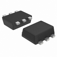
TRANS BR NPN/PNP DUAL 50V SOT563
Manufacturer
ON Semiconductor
Datasheet
1.NSBC143ZPDXV6T5.pdf
(14 pages)
Specifications of NSBC143ZPDXV6T5
Transistor Type
1 NPN, 1 PNP - Pre-Biased (Dual)
Current - Collector (ic) (max)
100mA
Voltage - Collector Emitter Breakdown (max)
50V
Resistor - Base (r1) (ohms)
4.7K
Resistor - Emitter Base (r2) (ohms)
47K
Dc Current Gain (hfe) (min) @ Ic, Vce
80 @ 5mA, 10V
Vce Saturation (max) @ Ib, Ic
250mV @ 1mA, 10mA
Current - Collector Cutoff (max)
500nA
Power - Max
500mW
Mounting Type
Surface Mount
Package / Case
SOT-563, SOT-6
Lead Free Status / RoHS Status
Contains lead / RoHS non-compliant
Frequency - Transition
-
Other names
NSBC143ZPDXV6T5OS


NSBC114EPDXV6T1,
NSBC114EPDXV6T5
Dual Bias Resistor
Transistors
NPN and PNP Silicon Surface Mount
Transistors with Monolithic Bias
Resistor Network
a monolithic bias network consisting of two resistors; a series base
resistor and a base−emitter resistor. These digital transistors are
designed to replace a single device and its external resistor bias
network. The BRT eliminates these individual components by
integrating them into a single device. In the NSBC114EPDXV6T1
series, two complementary BRT devices are housed in the SOT−563
package which is ideal for low power surface mount applications
where board space is at a premium.
MAXIMUM RATINGS
and Q
January, 2004 − Rev. 3
THERMAL CHARACTERISTICS
1. FR−4 @ Minimum Pad
Collector-Base Voltage
Collector-Emitter Voltage
Collector Current
Total Device Dissipation
Derate above 25 C
Thermal Resistance Junction-to-Ambient
Total Device Dissipation
Derate above 25 C
Thermal Resistance Junction-to-Ambient
Junction and Storage Temperature
The BRT (Bias Resistor Transistor) contains a single transistor with
Simplifies Circuit Design
Reduces Board Space
Reduces Component Count
Available in 8 mm, 7 inch Tape and Reel
Lead Free Solder Plating
Semiconductor Components Industries, LLC, 2004
2
, − minus sign for Q
(Both Junctions Heated)
(One Junction Heated)
Characteristic
Characteristic
Rating
(T
1
A
(PNP) omitted)
= 25 C unless otherwise noted, common for Q
Preferred Devices
T
T
A
A
= 25 C
= 25 C
Symbol
Symbol
Symbol
T
V
V
R
R
J
P
P
CBO
CEO
, T
I
qJA
qJA
C
D
D
stg
(Note 1)
(Note 1)
(Note 1)
(Note 1)
(Note 1)
(Note 1)
−55 to
Value
+150
Max
Max
100
357
350
500
250
2.9
4.0
50
50
1
mW/ C
mW/ C
mAdc
Unit
Unit
Unit
Vdc
Vdc
mW
mW
C/W
C/W
C
1
ORDERING INFORMATION
See specific marking information in the device marking table
on page 2 of this data sheet.
NSBC114EPDXV6T1 SOT−563
NSBC114EPDXV6T5 SOT−563
Preferred devices are recommended choices for future use
and best overall value.
Device
DEVICE MARKING INFORMATION
xx = Specific Device Code
D
(4)
(3)
Q
MARKING DIAGRAM
1
= Date Code
http://onsemi.com
(see table on page 2)
R
2
CASE 463A
SOT−563
PLASTIC
6
5 4
xx D
Package
(5)
R
1
Publication Order Number:
R
(2)
1
1
2 3
NSBC114EPDXV6/D
R
4000/Tape & Reel
8000/Tape & Reel
2
4 mm pitch
2 mm pitch
Shipping
(1)
Q
(6)
2
Related parts for NSBC143ZPDXV6T5
Image
Part Number
Description
Manufacturer
Datasheet
Request
R

Part Number:
Description:
ON Semiconductor [VOLTAGE REGULATOR]
Manufacturer:
ON Semiconductor
Datasheet:
Part Number:
Description:
357-036-542-201 CARDEDGE 36POS DL .156 BLK LOPRO
Manufacturer:
ON Semiconductor
Datasheet:
Part Number:
Description:
357-036-542-201 CARDEDGE 36POS DL .156 BLK LOPRO
Manufacturer:
ON Semiconductor
Datasheet:
Part Number:
Description:
357-036-542-201 CARDEDGE 36POS DL .156 BLK LOPRO
Manufacturer:
ON Semiconductor
Datasheet:
Part Number:
Description:
357-036-542-201 CARDEDGE 36POS DL .156 BLK LOPRO
Manufacturer:
ON Semiconductor
Datasheet:
Part Number:
Description:
357-036-542-201 CARDEDGE 36POS DL .156 BLK LOPRO
Manufacturer:
ON Semiconductor
Datasheet:
Part Number:
Description:
357-036-542-201 CARDEDGE 36POS DL .156 BLK LOPRO
Manufacturer:
ON Semiconductor
Datasheet:
Part Number:
Description:
357-036-542-201 CARDEDGE 36POS DL .156 BLK LOPRO
Manufacturer:
ON Semiconductor
Datasheet:
Part Number:
Description:
357-036-542-201 CARDEDGE 36POS DL .156 BLK LOPRO
Manufacturer:
ON Semiconductor
Datasheet:
Part Number:
Description:
357-036-542-201 CARDEDGE 36POS DL .156 BLK LOPRO
Manufacturer:
ON Semiconductor
Datasheet:
Part Number:
Description:
357-036-542-201 CARDEDGE 36POS DL .156 BLK LOPRO
Manufacturer:
ON Semiconductor
Datasheet:
Part Number:
Description:
Manufacturer:
ON Semiconductor
Datasheet:
Part Number:
Description:
Manufacturer:
ON Semiconductor
Datasheet:
Part Number:
Description:
Manufacturer:
ON Semiconductor
Datasheet: