PUML1,115 NXP Semiconductors, PUML1,115 Datasheet
PUML1,115
Specifications of PUML1,115


Related parts for PUML1,115


PUML1,115 Summary of contents
Page 1
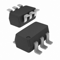
PUML1/ 200 mA NPN general-purpose transistor/ 100 mA NPN resistor-equipped transistor Rev. 01 — 14 July 2008 1. Product profile 1.1 General description NPN general-purpose transistor and NPN Resistor-Equipped Transistor (RET) in one SOT363 (SC-88) very small Surface-Mounted ...
Page 2
... NXP Semiconductors 2. Pinning information Table 2. Pin Ordering information Table 3. Type number PUML1/DG 4. Marking Table 4. Type number PUML1/DG [ made in Hong Kong * = p: made in Hong Kong * = t: made in Malaysia * = W: made in China 5. Limiting values Table 5. In accordance with the Absolute Maximum Rating System (IEC 60134). Symbol ...
Page 3
... NXP Semiconductors Table 5. In accordance with the Absolute Maximum Rating System (IEC 60134). Symbol P tot TR2 (resistor-equipped transistor) V CBO V CEO V EBO tot Per device P tot amb T stg [1] Device mounted on an FR4 Printed-Circuit Board (PCB), single-sided copper, tin-plated and standard footprint. Fig 1. ...
Page 4
... NXP Semiconductors 6. Thermal characteristics Table 6. Symbol Per transistor R th(j-a) Per device R th(j-a) [1] Device mounted on an FR4 PCB, single-sided copper, tin-plated and standard footprint duty cycle = 1 Z th(j-a) 0.75 ( K/W ) 0.5 0.33 2 0.2 10 0.1 0.05 0. FR4 PCB, standard footprint Fig 2. ...
Page 5
... NXP Semiconductors 7. Characteristics Table unless otherwise specified. amb Symbol Parameter TR1 (general-purpose transistor) I CBO I EBO CEsat TR2 (resistor-equipped transistor) I CBO I CEO I EBO CEsat V I(off) V I(on) R1 R2/ PUML1_DG_1 Product data sheet 50 V, 200 mA NPN general-purpose transistor/100 mA NPN RET Characteristics Conditions collector-base cut-off ...
Page 6
... NXP Semiconductors 500 h FE (1) 400 300 (2) 200 (3) 100 ( 150 C amb ( amb ( amb Fig 3. TR1: DC current gain as a function of collector current; typical values 1.3 V BEsat (V) (1) 0.9 (2) (3) 0 amb ( amb ( 150 C amb Fig 5. TR1: Base-emitter saturation voltage as a function of collector current; typical values ...
Page 7
... NXP Semiconductors ( 150 C amb ( amb ( amb Fig 7. TR2: DC current gain as a function of collector current; typical values 10 V I(on) (V) (1) ( amb ( amb ( 100 C amb Fig 9. TR2: On-state input voltage as a function of collector current; typical values PUML1_DG_1 Product data sheet 50 V, 200 mA NPN general-purpose transistor/100 mA NPN RET ...
Page 8
... NXP Semiconductors 8. Test information 8.1 Quality information This product has been qualified in accordance with the Automotive Electronics Council (AEC) standard Q101 - Stress test qualification for discrete semiconductors , and is suitable for use in automotive applications. 9. Package outline Fig 11. Package outline SOT363 (SC-88) 10 ...
Page 9
... NXP Semiconductors 11. Soldering Fig 12. Reflow soldering footprint SOT363 (SC-88) 4.5 Fig 13. Wave soldering footprint SOT363 (SC-88) PUML1_DG_1 Product data sheet 50 V, 200 mA NPN general-purpose transistor/100 mA NPN RET 2.65 1.5 2.35 0 1.8 1.3 1.3 2.45 5.3 Rev. 01 — 14 July 2008 PUML1/DG 0 ...
Page 10
... NXP Semiconductors 12. Revision history Table 9. Revision history Document ID Release date PUML1_DG_1 20080714 PUML1_DG_1 Product data sheet 50 V, 200 mA NPN general-purpose transistor/100 mA NPN RET Data sheet status Change notice Product data sheet - Rev. 01 — 14 July 2008 PUML1/DG Supersedes - © NXP B.V. 2008. All rights reserved. ...
Page 11
... Right to make changes — NXP Semiconductors reserves the right to make changes to information published in this document, including without limitation specifications and product descriptions, at any time and without notice ...
Page 12
... NXP Semiconductors 15. Contents 1 Product profi 1.1 General description 1.2 Features . . . . . . . . . . . . . . . . . . . . . . . . . . . . . . 1 1.3 Applications . . . . . . . . . . . . . . . . . . . . . . . . . . . 1 1.4 Quick reference data Pinning information . . . . . . . . . . . . . . . . . . . . . . 2 3 Ordering information . . . . . . . . . . . . . . . . . . . . . 2 4 Marking . . . . . . . . . . . . . . . . . . . . . . . . . . . . . . . . 2 5 Limiting values Thermal characteristics Characteristics . . . . . . . . . . . . . . . . . . . . . . . . . . 5 8 Test information . . . . . . . . . . . . . . . . . . . . . . . . . 8 8.1 Quality information . . . . . . . . . . . . . . . . . . . . . . 8 9 Package outline . . . . . . . . . . . . . . . . . . . . . . . . . 8 10 Packing information Soldering ...