PUMD48,125 NXP Semiconductors, PUMD48,125 Datasheet
PUMD48,125
Specifications of PUMD48,125


Related parts for PUMD48,125


PUMD48,125 Summary of contents
Page 1
PEMD48; PUMD48 NPN/PNP resistor-equipped transistors kΩ kΩ and R1 = 2.2 kΩ kΩ Rev. 05 — 13 April 2010 1. Product profile 1.1 General description NPN/PNP double Resistor-Equipped Transistors (RET) in ...
Page 2
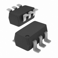
... NXP Semiconductors 2. Pinning information Table 3. Pin PEMD48 (SOT666 PUMD48 (SOT363 Ordering information Table 4. Type number Package PEMD48 PUMD48 4. Marking Table 5. Type number PEMD48 PUMD48 [ made in Hong Kong * = p: made in Hong Kong * = t: made in Malaysia * = W: made in China PEMD48_PUMD48_5 Product data sheet Pinning Description GND (emitter) TR1 ...
Page 3
... NXP Semiconductors 5. Limiting values Table 6. In accordance with the Absolute Maximum Rating System (IEC 60134). Symbol Per transistor; for the PNP transistor with negative polarity V CBO V CEO V EBO tot Per device P tot amb T stg [1] Device mounted on an FR4 Printed-Circuit Board (PCB), single-sided copper, tin-plated and standard footprint ...
Page 4
... NXP Semiconductors 6. Thermal characteristics Table 7. Symbol Per transistor R th(j-a) Per device R th(j-a) [1] Device mounted on an FR4 PCB, single-sided copper, tin-plated and standard footprint. [2] Reflow soldering is the only recommended soldering method. PEMD48_PUMD48_5 Product data sheet Thermal characteristics Parameter Conditions thermal resistance from ...
Page 5
... NXP Semiconductors 7. Characteristics Table amb Symbol Per transistor; for the PNP transistor with negative polarity I CBO I CEO Transistor TR1 (NPN) I EBO CEsat V I(off) V I(on) R1 R2/ Transistor TR2 (PNP) I EBO CEsat V I(off) V I(on) R1 R2/ PEMD48_PUMD48_5 Product data sheet Characteristics ° C unless otherwise specified. ...
Page 6
... NXP Semiconductors − 150 °C (1) T amb = 25 °C (2) T amb = −40 °C (3) T amb Fig 1. TR1 (NPN): DC current gain as a function of collector current; typical values I(on) (V) 10 (1) 1 (3) (2) −1 10 − 0 −40 °C (1) T amb = 25 °C (2) T amb = 100 °C (3) T amb Fig 3 ...
Page 7
... NXP Semiconductors −1 −10 −1 = − 150 °C (1) T amb = 25 °C (2) T amb = −40 °C (3) T amb Fig 5. TR2 (PNP): DC current gain as a function of collector current; typical values − I(on) (mV) −10 3 (1) (2) (3) −10 2 −1 −10 −1 = −0 −40 °C (1) T amb = 25 ° ...
Page 8
... NXP Semiconductors 8. Package outline 1.7 1 1.7 1.3 1.5 1.1 pin 1 index 1 2 0.5 1 Dimensions in mm Fig 9. Package outline PEMD48 (SOT666) 9. Packing information Table 9. The indicated -xxx are the last three digits of the 12NC ordering code. Type number PEMD48 PUMD48 [1] For further information and the availability of packing methods, see ...
Page 9
... Document ID Release date PEMD48_PUMD48_5 20100413 • Modifications: The format of this data sheet has been redesigned to comply with the new identity guidelines of NXP Semiconductors. • Legal texts have been adapted to the new company name where appropriate. • Section 1 “Product • Table 3 • ...
Page 10
... NXP Semiconductors and its customer, unless NXP Semiconductors and customer have explicitly agreed otherwise in writing event however, shall an agreement be valid in which the NXP Semiconductors product is deemed to offer functions and qualities beyond those described in the Product data sheet. ...
Page 11
... NXP Semiconductors 12. Contact information For more information, please visit: For sales office addresses, please send an email to: PEMD48_PUMD48_5 Product data sheet http://www.nxp.com salesaddresses@nxp.com All information provided in this document is subject to legal disclaimers. Rev. 05 — 13 April 2010 PEMD48; PUMD48 NPN/PNP resistor-equipped transistors © NXP B.V. 2010. All rights reserved. ...
Page 12
... NXP Semiconductors 13. Contents 1 Product profile . . . . . . . . . . . . . . . . . . . . . . . . . . 1 1.1 General description . . . . . . . . . . . . . . . . . . . . . 1 1.2 Features and benefits . . . . . . . . . . . . . . . . . . . . 1 1.3 Applications . . . . . . . . . . . . . . . . . . . . . . . . . . . 1 1.4 Quick reference data . . . . . . . . . . . . . . . . . . . . 1 2 Pinning information . . . . . . . . . . . . . . . . . . . . . . 2 3 Ordering information . . . . . . . . . . . . . . . . . . . . . 2 4 Marking . . . . . . . . . . . . . . . . . . . . . . . . . . . . . . . . 2 5 Limiting values Thermal characteristics . . . . . . . . . . . . . . . . . . 4 7 Characteristics . . . . . . . . . . . . . . . . . . . . . . . . . . 5 8 Package outline . . . . . . . . . . . . . . . . . . . . . . . . . 8 9 Packing information . . . . . . . . . . . . . . . . . . . . . 8 10 Revision history . . . . . . . . . . . . . . . . . . . . . . . . . 9 11 Legal information ...