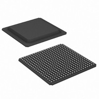
XC3S1600E-5FGG400C Xilinx Inc, XC3S1600E-5FGG400C Datasheet - Page 11

XC3S1600E-5FGG400C
Manufacturer Part Number
XC3S1600E-5FGG400C
Description
FPGA Spartan®-3E Family 1.6M Gates 33192 Cells 657MHz 90nm (CMOS) Technology 1.2V 400-Pin FBGA
Manufacturer
Xilinx Inc
Series
Spartan™-3Er
Datasheet
1.XC3S100E-4VQG100C.pdf
(233 pages)
Specifications of XC3S1600E-5FGG400C
Package
400FBGA
Family Name
Spartan®-3E
Device Logic Cells
33192
Device Logic Units
3688
Device System Gates
1600000
Number Of Registers
29504
Maximum Internal Frequency
657 MHz
Typical Operating Supply Voltage
1.2 V
Maximum Number Of User I/os
304
Ram Bits
663552
Number Of Logic Elements/cells
33192
Number Of Labs/clbs
3688
Total Ram Bits
663552
Number Of I /o
304
Number Of Gates
1600000
Voltage - Supply
1.14 V ~ 1.26 V
Mounting Type
Surface Mount
Operating Temperature
0°C ~ 85°C
Package / Case
400-BGA
Lead Free Status / RoHS Status
Lead free / RoHS Compliant
For Use With
HW-XA3S1600E-UNI-G - KIT DEVELOPMENT AUTOMOTIVE ECU
Lead Free Status / RoHS Status
Lead free / RoHS Compliant
Available stocks
Company
Part Number
Manufacturer
Quantity
Price
Company:
Part Number:
XC3S1600E-5FGG400C
Manufacturer:
XILINX
Quantity:
259
Company:
Part Number:
XC3S1600E-5FGG400C
Manufacturer:
Xilinx Inc
Quantity:
10 000
Part Number:
XC3S1600E-5FGG400C
Manufacturer:
XILINX/赛灵思
Quantity:
20 000
- Current page: 11 of 233
- Download datasheet (6Mb)
DS312-2 (v3.8) August 26, 2009
Product Specification
Notes:
1.
2.
IDDRIN1
IDDRIN2
OTCLK1
OTCLK2
ICLK1
ICLK2
IDDRIN1/IDDRIN2 signals shown with dashed lines connect to the adjacent IOB in a differential pair only, not to the FPGA fabric.
All IOB control and output path signals have an inverting polarity option wihtin the IOB.
TCE
OCE
REV
IQ1
ICE
IQ2
T1
T2
SR
O1
O2
T
I
R
D
CE
CK
D
CE
CK
D
CE
CK
D
CE
CK
D
CE
CK
D
CE
CK
SR
SR REV
SR
SR REV
SR
SR REV
REV
REV
REV
Q
Q
Q
Q
Q
Q
Figure 5: Simplified IOB Diagram
TFF1
TFF2
OFF1
OFF2
IFF1
IFF2
Programmable
Programmable
www.xilinx.com
DDR
MUX
DDR
MUX
Delay
Delay
Three-state Path
Input Path
Output Path
Program-
Output
mable
Driver
Single-ended Standards
LVCMOS, LVTTL, PCI
Differential Standards
using V REF
Functional Description
Pull-Up
Down
Pull-
Keeper
Latch
DS312-2_19_110606
V
Pin
I/O Pin
from
Adjacent
IOB
ESD
ESD
V
REF
CCO
I/O
Pin
11
Related parts for XC3S1600E-5FGG400C
Image
Part Number
Description
Manufacturer
Datasheet
Request
R

Part Number:
Description:
IC SPARTAN-3E FPGA 1600K 320-FBG
Manufacturer:
Xilinx Inc
Datasheet:

Part Number:
Description:
IC SPARTAN-3E FPGA 1600K 400FBGA
Manufacturer:
Xilinx Inc
Datasheet:

Part Number:
Description:
IC FPGA SPARTAN-3E 1600K 320FBGA
Manufacturer:
Xilinx Inc
Datasheet:

Part Number:
Description:
IC FPGA SPARTAN-3E 1600K 320FBGA
Manufacturer:
Xilinx Inc
Datasheet:

Part Number:
Description:
IC FPGA SPARTAN-3E 1600K 400FBGA
Manufacturer:
Xilinx Inc
Datasheet:

Part Number:
Description:
IC FPGA SPARTAN-3E 1600K 484FBGA
Manufacturer:
Xilinx Inc
Datasheet:

Part Number:
Description:
IC FPGA SPARTAN 3E 320FBGA
Manufacturer:
Xilinx Inc
Datasheet:

Part Number:
Description:
IC FPGA SPARTAN 3E 400FBGA
Manufacturer:
Xilinx Inc
Datasheet:

Part Number:
Description:
IC FPGA SPARTAN 3E 484FBGA
Manufacturer:
Xilinx Inc
Datasheet:

Part Number:
Description:
FPGA, SPARTAN-3E, 1600K GATES, 484FBGA
Manufacturer:
Xilinx Inc
Datasheet:

Part Number:
Description:
PROGRAMMABLE MICROCHIP
Manufacturer:
Xilinx Inc
Datasheet:

Part Number:
Description:
FPGA Spartan®-3E Family 1.6M Gates 33192 Cells 572MHz 90nm (CMOS) Technology 1.2V 484-Pin FBGA
Manufacturer:
Xilinx Inc
Datasheet:

Part Number:
Description:
FPGA Spartan®-3E Family 1.6M Gates 33192 Cells 657MHz 90nm (CMOS) Technology 1.2V 400-Pin FBGA
Manufacturer:
Xilinx Inc
Datasheet:

Part Number:
Description:
FPGA Spartan®-3E Family 1.6M Gates 33192 Cells 572MHz 90nm (CMOS) Technology 1.2V 320-Pin FBGA
Manufacturer:
Xilinx Inc
Datasheet:

Part Number:
Description:
IC CPLD .8K 36MCELL 44-VQFP
Manufacturer:
Xilinx Inc
Datasheet:


