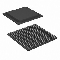
XC3S1600E-4FGG484I Xilinx Inc, XC3S1600E-4FGG484I Datasheet - Page 167

XC3S1600E-4FGG484I
Manufacturer Part Number
XC3S1600E-4FGG484I
Description
FPGA Spartan®-3E Family 1.6M Gates 33192 Cells 572MHz 90nm (CMOS) Technology 1.2V 484-Pin FBGA
Manufacturer
Xilinx Inc
Series
Spartan™-3Er
Datasheet
1.XC3S100E-4VQG100C.pdf
(233 pages)
Specifications of XC3S1600E-4FGG484I
Package
484FBGA
Family Name
Spartan®-3E
Device Logic Cells
33192
Device Logic Units
3688
Device System Gates
1600000
Number Of Registers
29504
Maximum Internal Frequency
572 MHz
Typical Operating Supply Voltage
1.2 V
Maximum Number Of User I/os
376
Ram Bits
663552
Number Of Logic Elements/cells
33192
Number Of Labs/clbs
3688
Total Ram Bits
663552
Number Of I /o
376
Number Of Gates
1600000
Voltage - Supply
1.14 V ~ 1.26 V
Mounting Type
Surface Mount
Operating Temperature
-40°C ~ 100°C
Package / Case
484-BBGA
Lead Free Status / RoHS Status
Lead free / RoHS Compliant
For Use With
HW-XA3S1600E-UNI-G - KIT DEVELOPMENT AUTOMOTIVE ECU
Lead Free Status / RoHS Status
Lead free / RoHS Compliant
Available stocks
Company
Part Number
Manufacturer
Quantity
Price
Company:
Part Number:
XC3S1600E-4FGG484I
Manufacturer:
XILINX
Quantity:
140
Company:
Part Number:
XC3S1600E-4FGG484I
Manufacturer:
XILINX
Quantity:
250
Company:
Part Number:
XC3S1600E-4FGG484I
Manufacturer:
Xilinx Inc
Quantity:
10 000
Part Number:
XC3S1600E-4FGG484I
Manufacturer:
XILINX/赛灵思
Quantity:
20 000
Table 129: Maximum User I/O by Package
Electronic versions of the package pinout tables and foot-
prints are available for download from the Xilinx website.
Download the files from the following location: Using a
spreadsheet program, the data can be sorted and reformat-
DS312-4 (v3.8) August 26, 2009
Product Specification
Notes:
1.
2.
XC3S100E
XC3S250E
XC3S500E
XC3S100E
XC3S250E
XC3S500E
XC3S100E
XC3S250E
XC3S250E
XC3S500E
XC3S250E
XC3S500E
XC3S1200E
XC3S500E
XC3S1200E
XC3S1600E
XC3S1200E
XC3S1600E
XC3S1600E
Device
Some VREF pins are on INPUT pins. See pinout tables for details.
All devices have 24 possible global clock and right- and left-half side clock inputs. The right-half and bottom-edge clock pins have shared
functionality in some FPGA configuration modes. Consequently, some clock pins are counted in the DUAL column. 4 GCLK pins, including
2 DUAL pins, are on INPUT pins.
R
Package
VQ100
CP132
TQ144
PQ208
FG320
FG400
FG484
FT256
Input-Only
Maximum
User I/Os
and
108
108
158
158
172
190
190
232
250
250
304
304
376
66
66
66
83
92
92
Maximum
Input-
Only
11
28
28
32
32
40
41
40
56
56
56
72
72
82
7
7
7
7
7
www.xilinx.com
Differential
Maximum
Pairs
124
124
156
30
30
30
35
41
41
40
40
65
65
68
77
77
92
99
99
ted according to any specific needs. Similarly, the
ASCII-text file is easily parsed by most scripting programs.
http://www.xilinx.com/support/documentation/data_sheets/s3e_pin.zip
102
120
120
156
156
214
I/O
16
16
16
16
22
22
22
20
58
58
62
76
78
INPUT
19
21
25
25
33
33
31
48
47
47
62
62
72
1
1
1
2
0
0
All Possible I/Os by Type
DUAL
21
21
21
42
46
46
42
42
46
46
46
46
46
46
46
46
46
46
46
VREF
13
13
15
19
19
20
21
21
24
24
28
4
4
4
7
8
8
9
9
)
Pinout Descriptions
(1
CLK
24
24
24
16
16
16
16
16
16
16
16
16
16
16
16
16
16
16
16
(2)
N.C.
16
18
0
0
0
9
0
0
0
0
0
0
0
0
0
0
0
0
0
167


