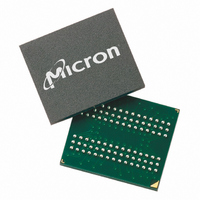
MT48LC4M32LFF5-8 IT:G Micron Technology Inc, MT48LC4M32LFF5-8 IT:G Datasheet - Page 31

MT48LC4M32LFF5-8 IT:G
Manufacturer Part Number
MT48LC4M32LFF5-8 IT:G
Description
DRAM Chip Mobile SDRAM 128M-Bit 4Mx32 3.3V 90-Pin VFBGA Tray
Manufacturer
Micron Technology Inc
Type
Mobile SDRAMr
Datasheet
1.MT48LC8M16LFB4-75MG_TR.pdf
(80 pages)
Specifications of MT48LC4M32LFF5-8 IT:G
Density
128 Mb
Maximum Clock Rate
125 MHz
Package
90VFBGA
Address Bus Width
14 Bit
Operating Supply Voltage
3.3 V
Maximum Random Access Time
19|8|7 ns
Operating Temperature
-40 to 85 °C
Format - Memory
RAM
Memory Type
Mobile SDRAM
Memory Size
128M (4Mx32)
Speed
125MHz
Interface
Parallel
Voltage - Supply
3 V ~ 3.6 V
Package / Case
90-VFBGA
Organization
4Mx32
Address Bus
14b
Access Time (max)
19/8/7ns
Operating Supply Voltage (typ)
3.3V
Package Type
VFBGA
Operating Temp Range
-40C to 85C
Operating Supply Voltage (max)
3.6V
Operating Supply Voltage (min)
3V
Supply Current
115mA
Pin Count
90
Mounting
Surface Mount
Operating Temperature Classification
Industrial
Lead Free Status / RoHS Status
Contains lead / RoHS non-compliant
Figure 16:
Figure 17:
PDF: 09005aef807f4885/Source: 09005aef8071a76b
128Mbx16x32Mobile_2.fm - Rev. M 1/09 EN
READ-to-WRITE
READ-to-WRITE with Extra Clock Cycle
Notes:
Notes:
COMMAND
1. CL = 3 is used for illustration.
2. The READ command may be to any bank, and the WRITE command may be to any bank.
3. If a burst of 1 is used, then DQM is not required.
The DQM input is used to avoid I/O contention, as shown in Figure 16 and Figure 17.
The DQM signal must be asserted (HIGH) at least 2 clocks prior to the WRITE command
(DQM latency is 2 clocks for output buffers) to suppress data-out from the READ. After
the WRITE command is registered, the DQ will go High-Z (or remain High-Z), regardless
of the state of the DQM signal, provided the DQM was active on the clock just prior to
the WRITE command that truncated the READ command. If not, the second WRITE will
be an invalid WRITE. For example, if DQM was LOW during T4 in Figure 17, then the
WRITEs at T5 and T7 would be valid, while the WRITE at T6 would be invalid.
The DQM signal must be de-asserted prior to the WRITE command (DQM latency is
0 clocks for input buffers) to ensure that the written data is not masked. Figure 16 shows
the case where the clock frequency allows for bus contention to be avoided without
adding a NOP cycle, and Figure 17 shows the case where the additional NOP is needed.
COMMAND
1. CL = 3 is used for illustration. The READ command may be to any bank, and the WRITE com-
ADDRESS
ADDRESS
mand may be to any bank.
DQM
DQM
CLK
CLK
DQ
DQ
BANK,
COL n
T0
BANK,
T0
COL n
READ
READ
TRANSITIONING DATA
T1
T1
NOP
NOP
T2
T2
TRANSITIONING DATA
NOP
NOP
31
T3
T3
NOP
NOP
D
t HZ
OUT
D
t HZ
OUT
t CK
Micron Technology, Inc., reserves the right to change products or specifications without notice.
n
n
DON’T CARE
T4
BANK,
COL b
T4
WRITE
NOP
D
IN
128Mb: x16, x32 Mobile SDRAM
b
t
DS
DON’T CARE
T5
BANK,
COL b
WRITE
D
IN
b
t
DS
©2001 Micron Technology, Inc. All rights reserved.
READs


