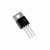
2N6508G ON Semiconductor, 2N6508G Datasheet - Page 3

2N6508G
Manufacturer Part Number
2N6508G
Description
THYRISTOR SCR 25A 600V TO220AB
Manufacturer
ON Semiconductor
Type
SCRr
Specifications of 2N6508G
Scr Type
Standard Recovery
Voltage - Off State
600V
Voltage - Gate Trigger (vgt) (max)
1.5V
Voltage - On State (vtm) (max)
1.8V
Current - On State (it (av)) (max)
16A
Current - On State (it (rms)) (max)
25A
Current - Gate Trigger (igt) (max)
30mA
Current - Hold (ih) (max)
40mA
Current - Off State (max)
10µA
Current - Non Rep. Surge 50, 60hz (itsm)
250A @ 60Hz
Operating Temperature
-40°C ~ 125°C
Mounting Type
Through Hole
Package / Case
TO-220-3 (Straight Leads)
Current - On State (it (rms) (max)
25A
Repetitive Peak Off-state Volt
600V
Off-state Voltage
600V
Average On-state Current
16A
Hold Current
40mA
Gate Trigger Current (max)
30mA
Gate Trigger Voltage (max)
1.5V
Package Type
TO-220AB
Peak Repeat Off Current
10uA
Peak Surge On-state Current (max)
250A
On State Voltage(max)
1.8@50AV
Mounting
Through Hole
Pin Count
3 +Tab
Operating Temp Range
-40C to 125C
Operating Temperature Classification
Automotive
Current, Forward
25 A
Current, Surge
250 A
Primary Type
SCR
Resistance, Thermal, Junction To Case
1.5 °C/W
Temperature, Junction, Maximum
+125 °C
Temperature, Operating
-40 to +125 °C
Voltage, Forward
1.8 V
Voltage, Reverse
600 V
Lead Free Status / RoHS Status
Lead free / RoHS Compliant
Other names
2N6508GOS
Available stocks
Company
Part Number
Manufacturer
Quantity
Price
Company:
Part Number:
2N6508G
Manufacturer:
TOSHIBA
Quantity:
30 000
Symbol
V
I
V
I
V
I
110
DRM
RRM
H
13
12
10
90
80
DRM
RRM
TM
0
0
0
0
Figure 1. Average Current Derating
Parameter
Peak Repetitive Off State Forward Voltage
Peak Forward Blocking Current
Peak Repetitive Off State Reverse Voltage
Peak Reverse Blocking Current
Peak On State Voltage
Holding Current
I
T(AV)
4.0
= 30
, ON‐STATE FORWARD CURRENT (AMPS)
8.0
60
90
Voltage Current Characteristic of SCR
12
= CONDUCTION ANGLE
180
16
http://onsemi.com
2N6504 Series
dc
I
Reverse Avalanche Region
Anode -
RRM
20
Reverse Blocking Region
3
at V
RRM
8.0
32
24
16
(off state)
0
0
Figure 2. Maximum On-State Power Dissipation
= CONDUCTION ANGLE
I
T(AV)
on state
, AVERAGE ON‐STATE FORWARD CURRENT (AMPS)
4.0
+ Current
= 30
Forward Blocking Region
I
H
8.0
V
60
TM
(off state)
90
I
DRM
12
Anode +
at V
DRM
T
J
+ Voltage
= 125 C
16
180
dc
20


