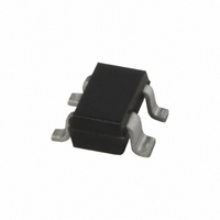
BFG10W/X,115 NXP Semiconductors, BFG10W/X,115 Datasheet - Page 3

BFG10W/X,115
Manufacturer Part Number
BFG10W/X,115
Description
TRANS NPN 10V 250MA SOT343N
Manufacturer
NXP Semiconductors
Datasheet
1.BFG10WX115.pdf
(11 pages)
Specifications of BFG10W/X,115
Package / Case
SOT-343N
Transistor Type
NPN
Voltage - Collector Emitter Breakdown (max)
10V
Frequency - Transition
1.9GHz
Power - Max
400mW
Dc Current Gain (hfe) (min) @ Ic, Vce
25 @ 50mA, 5V
Current - Collector (ic) (max)
250mA
Mounting Type
Surface Mount
Dc Current Gain Hfe Max
25 @ 50mA @ 5V
Mounting Style
SMD/SMT
Configuration
Single
Transistor Polarity
NPN
Collector- Emitter Voltage Vceo Max
10 V
Emitter- Base Voltage Vebo
2.5 V
Continuous Collector Current
0.25 A
Power Dissipation
400 mW
Maximum Operating Temperature
+ 175 C
Lead Free Status / RoHS Status
Lead free / RoHS Compliant
Gain
-
Noise Figure (db Typ @ F)
-
Lead Free Status / Rohs Status
Lead free / RoHS Compliant
Other names
934036590115
BFG10W/X T/R
BFG10W/X T/R
BFG10W/X T/R
BFG10W/X T/R
NXP Semiconductors
CHARACTERISTICS
T
1995 Sep 22
handbook, full pagewidth
V
V
V
I
h
C
C
SYMBOL
j
CES
FE
= 25 C (unless otherwise specified).
(BR)CBO
(BR)CEO
(BR)EBO
UHF power transistor
c
re
Z th j-a
(K/W)
Fig.2 Transient thermal impedance from junction to soldering point as a function of pulse time; typical values.
10
10
10
1
10
3
2
−6
collector-base breakdown voltage
collector-emitter breakdown voltage
emitter-base breakdown voltage
collector cut-off current
DC current gain
collector capacitance
feedback capacitance
δ = 1
0.75
0.33
0.05
0.02
0.01
0.5
0.2
0.1
PARAMETER
10
−5
10
−4
open base; I
open emitter; I
open collector; I
V
I
I
I
C
E
C
CE
= 50 mA; V
= i
= 0; V
= 6 V; V
e
= 0; V
10
3
CE
−3
CONDITIONS
= 6 V; f = 1 MHz
C
CB
BE
CE
= 5 mA
C
= 0
= 6 V; f = 1 MHz
E
= 0.1 mA
= 5 V
= 0.1 mA
10
−2
P
20
10
2.5
25
MIN.
10
t p
−1
T
Product specification
δ
BFG10W/X
100
3
2
=
t p (s)
MAX.
t p
T
t
MBG431
1
V
V
V
A
pF
pF
UNIT


