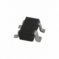
BFG520W,115 NXP Semiconductors, BFG520W,115 Datasheet - Page 6

BFG520W,115
Manufacturer Part Number
BFG520W,115
Description
TRANS NPN 6V 70MA SOT343N
Manufacturer
NXP Semiconductors
Datasheet
1.BFG520WX115.pdf
(15 pages)
Specifications of BFG520W,115
Package / Case
SOT-343N
Transistor Type
NPN
Voltage - Collector Emitter Breakdown (max)
15V
Frequency - Transition
9GHz
Noise Figure (db Typ @ F)
1.1dB ~ 2.1dB @ 900MHz
Power - Max
500mW
Dc Current Gain (hfe) (min) @ Ic, Vce
60 @ 20mA, 6V
Current - Collector (ic) (max)
70mA
Mounting Type
Surface Mount
Dc Collector/base Gain Hfe Min
60
Dc Current Gain Hfe Max
60 @ 20mA @ 6V
Mounting Style
SMD/SMT
Configuration
Dual
Transistor Polarity
NPN
Maximum Operating Frequency
9000 MHz (Typ)
Collector- Emitter Voltage Vceo Max
15 V
Emitter- Base Voltage Vebo
2.5 V
Continuous Collector Current
70 mA
Power Dissipation
500 mW
Maximum Operating Temperature
+ 175 C
Lead Free Status / RoHS Status
Lead free / RoHS Compliant
Gain
-
Lead Free Status / Rohs Status
Lead free / RoHS Compliant
Other names
934030630115
BFG520W T/R
BFG520W T/R
BFG520W T/R
BFG520W T/R
NXP Semiconductors
handbook, halfpage
handbook, halfpage
NPN 9 GHz wideband transistors
I
f = 900 MHz; V
C
(dB)
gain
gain
(dB)
= 5 mA; V
Fig.6
30
20
10
50
40
30
20
10
0
0
10
Fig.8
0
MSG
CE
G UM
MSG
Gain as a function of collector current;
typical values.
= 6 V.
CE
Gain as a function of frequency;
typical values.
= 6 V.
10
10
2
20
10
3
30
f (MHz)
G max
G
I
G max
UM
C
(mA)
MLB810
MLB812
10
Rev. 04 - 21 November 2007
40
4
handbook, halfpage
handbook, halfpage
f = 2 GHz; V
I
(dB)
gain
C
gain
(dB)
= 20 mA; V
Fig.7
50
40
30
20
10
0
30
20
10
10
Fig.9
0
0
MSG
CE
G UM
MSG
CE
Gain as a function of collector current;
typical values.
= 6 V.
= 6 V.
Gain as a function of frequency;
typical values.
BFG520W; BFG520W/X
10
10
2
20
10
3
Product specification
30
f (MHz)
G max
G max
G
I
UM
C
MLB813
(mA)
MLB811
6 of 15
10
40
4


