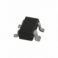
BFG540W/X,115 NXP Semiconductors, BFG540W/X,115 Datasheet - Page 9

BFG540W/X,115
Manufacturer Part Number
BFG540W/X,115
Description
TRANS WIDEBAND 9GHZ SOT-343 15V
Manufacturer
NXP Semiconductors
Datasheet
1.BFG540WX115.pdf
(17 pages)
Specifications of BFG540W/X,115
Package / Case
SOT-343N
Mounting Type
Surface Mount
Power - Max
500mW
Current - Collector (ic) (max)
120mA
Voltage - Collector Emitter Breakdown (max)
15V
Gain
16dB
Transistor Type
NPN
Frequency - Transition
9GHz
Dc Current Gain (hfe) (min) @ Ic, Vce
100 @ 40mA, 8V
Noise Figure (db Typ @ F)
2.1dB @ 2GHz
Dc Current Gain Hfe Max
100 @ 40mA @ 8V
Mounting Style
SMD/SMT
Configuration
Single
Transistor Polarity
NPN
Maximum Operating Frequency
9000 MHz (Typ)
Collector- Emitter Voltage Vceo Max
15 V
Emitter- Base Voltage Vebo
2.5 V
Continuous Collector Current
0.12 A
Power Dissipation
500 mW
Maximum Operating Temperature
+ 175 C
Lead Free Status / Rohs Status
Lead free / RoHS Compliant
Other names
934032320115::BFG540W/X T/R::BFG540W/X T/R::Q2638421
NXP Semiconductors
2000 May 23
handbook, full pagewidth
handbook, full pagewidth
NPN 9 GHz wideband transistor
f = 900 MHz; V
f = 2 GHz; V
CE
CE
= 8 V; I
= 8 V; I
C
= 10 mA; Z
C
= 10 mA; Z
unstable
region
180
180
Fig.17 Common emitter noise figure circles; typical values.
Fig.18 Common emitter noise figure circles; typical values.
o
= 50
o
o
o
= 50
0
0
G
135
135
135
max
135
0.2
0.2
0.2
0.2
o
o
o
o
= 9.8 dB
0.2
0.2
Γ
opt
0.5
0.5
0.5
0.5
F = 1.5 dB
F = 3 dB
G = 9 dB G = 8 dB
F = 4 dB
F = 1.5 dB
0.5
0.5
F
F
F = 3 dB
F = 2 dB
min
min
= 2.1 dB
= 1.3 dB
Γ
opt
9
90
90
90
90
1
1
1
1
1
1
o
o
o
o
stability
circle
2
2
BFG540W/X; BFG540W/XR
2
2
2
2
5
5
45
45
45
45
o
o
o
o
5
5
5
5
MLC051
MLC052
0
0
o
o
1.0
0.8
0.6
0.4
0.2
0
1.0
1.0
0.8
0.6
0.4
0.2
0
1.0
Product specification
BFG540W


