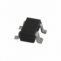
BFG540W/X,115 NXP Semiconductors, BFG540W/X,115 Datasheet - Page 3

BFG540W/X,115
Manufacturer Part Number
BFG540W/X,115
Description
TRANS WIDEBAND 9GHZ SOT-343 15V
Manufacturer
NXP Semiconductors
Datasheet
1.BFG540WX115.pdf
(17 pages)
Specifications of BFG540W/X,115
Package / Case
SOT-343N
Mounting Type
Surface Mount
Power - Max
500mW
Current - Collector (ic) (max)
120mA
Voltage - Collector Emitter Breakdown (max)
15V
Gain
16dB
Transistor Type
NPN
Frequency - Transition
9GHz
Dc Current Gain (hfe) (min) @ Ic, Vce
100 @ 40mA, 8V
Noise Figure (db Typ @ F)
2.1dB @ 2GHz
Dc Current Gain Hfe Max
100 @ 40mA @ 8V
Mounting Style
SMD/SMT
Configuration
Single
Transistor Polarity
NPN
Maximum Operating Frequency
9000 MHz (Typ)
Collector- Emitter Voltage Vceo Max
15 V
Emitter- Base Voltage Vebo
2.5 V
Continuous Collector Current
0.12 A
Power Dissipation
500 mW
Maximum Operating Temperature
+ 175 C
Lead Free Status / Rohs Status
Lead free / RoHS Compliant
Other names
934032320115::BFG540W/X T/R::BFG540W/X T/R::Q2638421
NXP Semiconductors
LIMITING VALUES
In accordance with the Absolute Maximum Rating System (IEC 60134).
Note
1. T
THERMAL CHARACTERISTICS
Note
1. T
2000 May 23
handbook, halfpage
V
V
V
I
P
T
T
R
SYMBOL
SYMBOL
C
stg
j
CBO
CES
EBO
tot
NPN 9 GHz wideband transistor
th j-s
(mW)
V
P tot
CE
s
s
600
400
200
is the temperature at the soldering point of the collector pin.
is the temperature at the soldering point of the collector pin.
10 V.
0
0
collector-base voltage
collector-emitter voltage
emitter-base voltage
collector current (DC)
total power dissipation
storage temperature
junction temperature
thermal resistance from junction to soldering point
Fig.3 Power derating curve.
50
PARAMETER
100
PARAMETER
150
T
s
MBG248
( C)
o
open emitter
R
open collector
T
s
BE
200
85 C; see Fig.3; note 1
= 0
CONDITIONS
3
T
s
85 C; note 1
CONDITIONS
BFG540W/X; BFG540W/XR
65
MIN.
20
15
2.5
120
500
+150
175
VALUE
Product specification
MAX.
180
BFG540W
V
V
V
mA
mW
C
C
UNIT
UNIT
K/W


