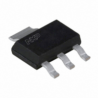
BFG541,115 NXP Semiconductors, BFG541,115 Datasheet - Page 8

BFG541,115
Manufacturer Part Number
BFG541,115
Description
TRANS NPN 15V 9GHZ SOT223
Manufacturer
NXP Semiconductors
Datasheet
1.BFG541115.pdf
(14 pages)
Specifications of BFG541,115
Package / Case
SOT-223 (3 leads + Tab), SC-73, TO-261
Transistor Type
NPN
Voltage - Collector Emitter Breakdown (max)
15V
Frequency - Transition
9GHz
Noise Figure (db Typ @ F)
1.3dB ~ 2.4dB @ 900MHz
Power - Max
650mW
Dc Current Gain (hfe) (min) @ Ic, Vce
60 @ 40mA, 8V
Current - Collector (ic) (max)
120mA
Mounting Type
Surface Mount
Dc Current Gain Hfe Max
60 @ 40mA @ 8V
Mounting Style
SMD/SMT
Configuration
Single Dual Emitter
Transistor Polarity
NPN
Maximum Operating Frequency
9000 MHz (Typ)
Collector- Emitter Voltage Vceo Max
15 V
Emitter- Base Voltage Vebo
2.5 V
Continuous Collector Current
0.12 A
Power Dissipation
650 mW
Maximum Operating Temperature
+ 175 C
Dc
08+
Lead Free Status / RoHS Status
Lead free / RoHS Compliant
Gain
-
Lead Free Status / Rohs Status
Lead free / RoHS Compliant
Other names
568-1984-2
934018870115
BFG541 T/R
934018870115
BFG541 T/R
NXP Semiconductors
September 1995
handbook, full pagewidth
handbook, full pagewidth
NPN 9 GHz wideband transistor
I
Z
I
Z
C
C
o
o
= 10 mA; V
= 10 mA; V
= 50 ; f = 900 MHz.
= 50 ; f = 2 GHz.
CE
CE
= 8 V;
= 8 V;
180°
180°
G max = 15.3 dB
0
0
−135°
−135°
G = 15 dB
135°
135°
0.2
0.2
0.2
0.2
Γ MS
G = 14 dB
0.2
0.2
G max = 8.5 dB
F min = 2.1 dB
G = 13 dB
0.5
0.5
0.5
0.5
Γ MS
Fig.14 Noise circle figure.
Fig.15 Noise circle figure.
Γ OPT
F = 2.5 dB
0.5
0.5
G = 8 dB
F = 3 dB
F = 1.5 dB
F min =
1.3 dB
G = 7 dB
Γ OPT
F = 4 dB
F = 2 dB
−90°
−90°
90°
90°
8
1
1
F = 3 dB
1
1
1
1
G = 6 dB
2
2
2
2
2
2
5
5
−45°
−45°
45°
45°
5
5
5
5
MRA668
MRA669
0°
0°
1.0
0.8
0.6
0.4
0.2
0
1.0
1.0
0.8
0.6
0.4
0.2
0
1.0
Product specification
BFG541


