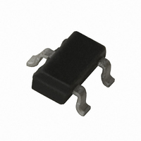
AT-32033-TR1G Avago Technologies US Inc., AT-32033-TR1G Datasheet - Page 2

AT-32033-TR1G
Manufacturer Part Number
AT-32033-TR1G
Description
IC TRANS NPN BIPOLAR SOT-23
Manufacturer
Avago Technologies US Inc.
Specifications of AT-32033-TR1G
Transistor Type
NPN
Voltage - Collector Emitter Breakdown (max)
5.5V
Noise Figure (db Typ @ F)
1dB ~ 1.3dB @ 900MHz
Gain
11dB ~ 12.5dB
Power - Max
200mW
Dc Current Gain (hfe) (min) @ Ic, Vce
70 @ 2mA, 2.7V
Current - Collector (ic) (max)
32mA
Mounting Type
Surface Mount
Package / Case
SOT-23-3, TO-236-3, Micro3™, SSD3, SST3
Transistor Polarity
NPN
Collector Emitter Voltage V(br)ceo
5.5V
Transition Frequency Typ Ft
10GHz
Power Dissipation Pd
200mW
Dc Collector Current
32mA
Dc Current Gain Hfe
70
Lead Free Status / RoHS Status
Lead free / RoHS Compliant
Frequency - Transition
-
Lead Free Status / RoHS Status
Lead free / RoHS Compliant, Lead free / RoHS Compliant
Other names
516-1566-2
Available stocks
Company
Part Number
Manufacturer
Quantity
Price
Company:
Part Number:
AT-32033-TR1G
Manufacturer:
TI
Quantity:
2 906
Part Number:
AT-32033-TR1G
Manufacturer:
AVAGO/安华高
Quantity:
20 000
AT-32011, AT-32033 Absolute Maximum Ratings
Electrical Specifications, T
Notes:
1. Test circuit A, Figure 1. Numbers reflect device performance de-embedded from circuit losses. Input loss = 0.3 dB;
2. Test circuit B, Figure 1. Numbers reflect device performance de-embedded from circuit losses. Input loss = 0.3 dB;
Figure 1. Test Circuit for Noise Figure and Associated Gain.
This circuit is a compromise match between best noise figure, best gain, stability, and a practical
synthesizable match.
1000 pF
Symbol
RF IN
TEST CIRCUIT
BOARD MATL = 0.062" FR-4 (ε = 4.8)
DIMENSIONS IN MILS
output loss = 0.3 dB.
output loss = 0.3 dB.
Symbol
I
I
V
V
V
T
NF
G
h
CBO
EBO
P
EBO
CBO
CEO
I
T
STG
FE
A
C
T
j
W = 10
CKT A: L = 380
CKT B: L = 380
V
BB
Noise Figure
Associated Gain
Forward Current Transfer Ratio
Collector Cutoff Current
Emitter Cutoff Current
V
V
V
V
V
Parameters and Test Conditions
CE
CE
CB
CE
EB
W = 10 L = 1870
Emitter-Base Voltage
Collector-Base Voltage
Collector-Emitter Voltage
Collector Current
Power Dissipation
Junction Temperature
Storage Temperature
= 2.7 V, I
= 2.7 V, I
= 3 V
= 2.7 V, I
= 1 V
Parameter
C
C
C
= 2 mA
= 2 mA
= 2 mA
W = 30
L = 60
[2, 3]
A
= 25
f = 0.9 GHz
f = 0.9 GHz
CKT A: W = 30 L = 50 x 2
CKT B: W = 30 L = 60
W = 30
L = 60
°
C
Units
mW
mA
°C
°C
V
V
V
W = 10 L = 1870
NOT TO SCALE
Units
µA
µA
dB
dB
–
Maximum
Absolute
-65 to 150
V
200
150
W = 10
CKT A: L = 105
CKT B: L = 850
1.5
5.5
CC
11
32
12.5
Min.
70
CKT A: 25 Ω
CKT B: 5 Ω
[1]
[1]
AT-32011
Typ.
1.0
14
1000 pF
[1]
[1]
RF OUT
Notes:
1. Operation of this device above any one
of these parameters may cause permanent
damage.
2. T
3. Derate at 1.82 mW/°C for T
Mounting Surface
Max.
1.3
300
0.2
1.5
2
Thermal Resistance
[1]
θ
jc
Min.
11
70
= 550 °C/W
= 25°C.
[2]
AT-32033
12.5
Typ.
1.0
[2]
C
[2]
> 40°C.
[2]
Max.
1.3
:
300
0.2
1.5
[2]


