AT-32033-TR1G Avago Technologies US Inc., AT-32033-TR1G Datasheet
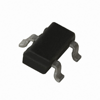
IC TRANS NPN BIPOLAR SOT-23

AT-32033-TR1G

Manufacturer Part Number
AT-32033-TR1G
Description
IC TRANS NPN BIPOLAR SOT-23
Manufacturer
Avago Technologies US Inc.
Datasheets

Specifications of AT-32033-TR1G

Transistor Type
NPN
Voltage - Collector Emitter Breakdown (max)
5.5V
Noise Figure (db Typ @ F)
1dB ~ 1.3dB @ 900MHz
Gain
11dB ~ 12.5dB
Power - Max
200mW
Dc Current Gain (hfe) (min) @ Ic, Vce
70 @ 2mA, 2.7V
Current - Collector (ic) (max)
32mA
Mounting Type
Surface Mount
Package / Case
SOT-23-3, TO-236-3, Micro3™, SSD3, SST3
Transistor Polarity
NPN
Collector Emitter Voltage V(br)ceo
5.5V
Transition Frequency Typ Ft
10GHz
Power Dissipation Pd
200mW
Dc Collector Current
32mA
Dc Current Gain Hfe
70
Lead Free Status / RoHS Status
Lead free / RoHS Compliant
Frequency - Transition
-
Lead Free Status / RoHS Status
Lead free / RoHS Compliant, Lead free / RoHS Compliant
Other names
516-1566-2

Available stocks

Company
Part Number
Manufacturer
Quantity
Price
Part Number:
AT-32033-TR1G
Manufacturer:
TI
Quantity:
2 906
Part Number:
AT-32033-TR1G
Manufacturer:
AVAGO/安华高
Quantity:
20 000
Company:
Part Number:
AT-32033-TR1G
Quantity:
229
AT-32011, AT-32033
Low Current, High Performance NPN
Silicon Bipolar Transistor
Data Sheet
Description
Avago’s AT-32011 and AT-32033 are high performance
NPN bipolar transistors that have been optimized for
maximum f
for use in battery powered applications in wireless mar-
kets. The AT-32033 uses the 3 lead SOT-23, while the AT-
32011 places the same die in the higher performance 4
lead SOT-143. Both packages are industry standard, and
compatible with high volume surface mount assembly
techniques.
The 3.2 micron emitter-to-emitter pitch and reduced
parasitic design of these transistors yields extremely high
performance products that can perform a multiplicity
of tasks. The 20 emitter finger interdigitated geometry
yields an easy to match to and extremely fast transistor
with moderate power, low noise resistance, and low op-
erating currents.
Optimized performance at 2.7 V makes these devices
ideal for use in 900 MHz, 1.8 GHz, and 2.4 GHz battery
operated systems as an LNA, gain stage, buffer, oscilla-
tor, or active mixer. Typical amplifier designs at 900 MHz
yield 1.2 dB noise figures with 12 dB or more associated
gain at a 2.7 V, 2 mA bias, with noise performance being
relatively insensitive to input match. High gain capabil-
ity at 1 V, 1 mA makes these devices a good fit for 900
MHz pager applications. Voltage breakdowns are high
enough for use at 5 volts.
The AT-3 series bipolar transistors are fabricated using
an optimized version of Avago’s 10 GHz f
Self-Aligned-Transistor (SAT) process. The die are nitride
passivated for surface protection. Excellent device uni-
formity, performance and reliability are produced by the
use of ion-implantation, self-alignment techniques, and
gold metalization in the fabrication of these devices.
t
at low voltage operation, making them ideal
t
, 30 GHz f
MAX
Features
• High Performance Bipolar Transistor Optimized for
• 900 MHz Performance:
• Characterized for End-Of-Life Battery Use (2.7 V)
• SOT-23 and SOT-143 SMT Plastic Packages
• Tape-And-Reel Packaging Option Available
• Lead-free
Pin Connections and Package Marking
Notes:
Top View. Package Marking provides orientation and identification.
"x" is the date code.
Low Current, Low Voltage Operation
AT-32011: 1 dB NF, 14 dB G
AT-32033: 1 dB NF, 12.5 dB G
EMITTER COLLECTOR
SOT-143 (AT-32011)
SOT-23 (AT-32033)
BASE
BASE
Note:
Top view. Package marking provides orientation
and identification. "x" is the date code.
COLLECTOR
320x
320x
EMITTER
EMITTER
A
A

Related parts for AT-32033-TR1G

AT-32033-TR1G Summary of contents

Page 1

... bias, with noise performance being relatively insensitive to input match. High gain capabil- ity makes these devices a good fit for 900 MHz pager applications. Voltage breakdowns are high enough for use at 5 volts. ...

Page 2

... CKT 380 CKT 380 TEST CIRCUIT BOARD MATL = 0.062" FR-4 (ε = 4.8) DIMENSIONS IN MILS Figure 1. Test Circuit for Noise Figure and Associated Gain. This circuit is a compromise match between best noise figure, best gain, stability, and a practical synthesizable match. 2 Absolute Units Maximum V 1 ...

Page 3

... Figure 2. AT-32011 and AT-32033 Minimum Noise Fig- ure vs. Frequency and Current 2 AT-32011 fig 0.5 1.0 1.5 2.0 2.5 FREQUENCY (GHz) Figure 5. AT-32011 and AT-32033 Power Gain Compression vs. Frequency and Current 2 AT-32011 fig 0.9 GHz f = 0.9 GHz f = 0.9 GHz f = 0.9 GHz 0.5 1 ...

Page 4

... FREQUENCY (GHz) Figure 8. AT-32011 and AT-32033 Power Gain Compression vs. Frequency and Current AT-32011 fig 7.5 5 2 0.5 1.0 1.5 2.0 2.5 FREQUENCY (GHz) Figure 11. AT-32011 and AT-32033 Power Gain Compression vs. Frequency and Current AT-32011 fig 11 25 2 1 100 TEMPERATURE (° ...

Page 5

... F               min GHz dB 0.5 [1] 0.42 0.9 0.71 1.8 1.37 2.4 1.80 Note: 1. 0.5 GHz noise parameter values are extrapolated, not measured. AT-32033 Typical Scattering Parameters, Freq GHz Mag Ang 0.1 0.97 -11 0.5 0.81 -52 0.9 0.61 -87 1 ...

Page 6

... Freq. F min GHz dB 0.5 [1] 0.57 0.9 0.78 1.8 1.25 2.4 1.57 Note: 1. 0.5 GHz noise parameter values are extrapolated, not measured. AT-32033 Typical Scattering Parameters, Freq GHz Mag Ang 0.1 0.93 -13 0.5 0.68 -56 0.9 0.44 -86 1 ...

Page 7

... Freq. F min GHz dB 0.5 [1] 1.39 0.9 1.51 1.8 1.78 2.4 1.96 Note: 1. 0.5 GHz noise parameter values are extrapolated, not measured. AT-32033 Typical Scattering Parameters, Freq GHz Mag Ang 0.1 0.50 -35 0.5 0.16 -52 0.9 0.08 -36 1 ...

Page 8

... Freq. F min GHz dB 0.5 [1] 0.52 0.9 0.75 1.8 1.26 2.4 1.60 Note: 1. 0.5 GHz noise parameter values are extrapolated, not measured. AT-32033 Typical Scattering Parameters, Freq GHz Mag Ang 0.1 0.94 -13 0.5 0.69 -54 0.9 0.45 -82 1 ...

Page 9

... Freq. F min GHz dB 0.5 [1] 1.38 0.9 1.50 1.8 1.78 2.4 1.96 Note: 1. 0.5 GHz noise parameter values are extrapolated, not measured. AT-32033 Typical Scattering Parameters, Freq GHz Mag Ang 0.1 0.55 -31 0.5 0.20 -44 0.9 0.13 -31 1 ...

Page 10

... Ordering Information Part Numbers No. of Devices AT-32011-BLKG AT-32033-BLKG AT-32011-TR1G AT-32033-TR1G AT-32011-TR2G AT-32033-TR2G Package Dimensions SOT-23 Plastic Package e2 e1 XXX SYMBOL Notes: e2 XXX-package marking Drawings are not to scale For product information and a complete list of distributors, please go to our web site: Avago, Avago Technologies, and the A logo are trademarks of Avago Technologies in the United States and other countries. ...

Related keywords