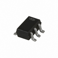
BF1205C,115 NXP Semiconductors, BF1205C,115 Datasheet - Page 14

BF1205C,115
Manufacturer Part Number
BF1205C,115
Description
MOSFET N-CH DUAL GATE 10V SOT363
Manufacturer
NXP Semiconductors
Datasheet
1.BF1205C115.pdf
(22 pages)
Specifications of BF1205C,115
Package / Case
SC-70-6, SC-88, SOT-363
Transistor Type
N-Channel Dual Gate
Frequency
400MHz
Gain
30dB
Voltage - Rated
6V
Current Rating
30mA
Noise Figure
1.3dB
Current - Test
19mA
Voltage - Test
5V
Configuration
Dual
Continuous Drain Current
30 mA
Drain-source Breakdown Voltage
6 V
Gate-source Breakdown Voltage
6 V
Maximum Operating Temperature
+ 150 C
Minimum Operating Temperature
- 65 C
Mounting Style
SMD/SMT
Power Dissipation
180 mW
Transistor Polarity
N-Channel
Application
VHF/UHF
Channel Type
N
Channel Mode
Enhancement
Drain Source Voltage (max)
6V
Power Gain (typ)@vds
35@5VdB
Noise Figure (max)
2.1dB
Package Type
SOT-363
Pin Count
6
Input Capacitance (typ)@vds
2.2@5V@Gate 1@Amp A/3@5V@Gate 2@Amp A/2@5V@Gate 1@Amp B/3.4@5V@Gate 2@Amp BpF
Output Capacitance (typ)@vds
0.9@5V@Amp A/0.85@5V@Amp BpF
Reverse Capacitance (typ)
0.02@5VpF
Operating Temp Range
-65C to 150C
Mounting
Surface Mount
Number Of Elements
2
Power Dissipation (max)
180mW
Screening Level
Military
Lead Free Status / RoHS Status
Lead free / RoHS Compliant
Power - Output
-
Lead Free Status / Rohs Status
Lead free / RoHS Compliant
Other names
934058083115
BF1205C T/R
BF1205C T/R
BF1205C T/R
BF1205C T/R
Philips Semiconductors
BF1205C_2
Product data sheet
Fig 23. Drain current as a function of gate 1 (V
(mA)
(1) R
(2) R
(3) R
(4) R
(5) R
(6) R
(7) R
(8) R
I
D
24
16
8
0
V
R
drain supply voltage and value of RG1; typical
values.
0
G2-S
G1(b)
G1(b)
G1(b)
G1(b)
G1(b)
G1(b)
G1(b)
G1(b)
G1(b)
= 4 V; V
= 68 k .
= 82 k .
= 100 k .
= 120 k .
= 150 k .
= 180 k .
= 220 k .
= 270 k .
is connected to V
DS(a)
2
= V
G1-S(a)
GG
; see
= 0 V; T
4
Figure
V
GG
j
= 25 C;
001aaa574
V
3.
(1)
(2)
(3)
(4)
(5)
(6)
(7)
(8)
DS
(V)
Rev. 02 — 15 August 2006
6
GG
),
Fig 24. Drain current as a function of gate 2 voltage;
(mA)
(1) V
(2) V
(3) V
(4) V
(5) V
I
D
16
12
8
4
0
V
R
typical values.
0
GG
GG
GG
GG
GG
DS(b)
G1(b)
= 5.0 V.
= 4.5 V.
= 4.0 V.
= 3.5 V.
= 3.0 V.
= 5 V; V
= 150 k (connected to V
Dual N-channel dual gate MOS-FET
DS(a)
2
= V
© Koninklijke Philips Electronics N.V. 2006. All rights reserved.
G1-S(a)
= 0 V; T
4
GG
); see
BF1205C
V
G2-S
j
001aaa575
= 25 C;
(1)
(2)
(3)
(4)
(5)
(V)
Figure
6
3.
14 of 22


