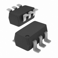
BF1210,115 NXP Semiconductors, BF1210,115 Datasheet - Page 2

BF1210,115
Manufacturer Part Number
BF1210,115
Description
MOSFET N-CH DUAL GATE 6V UMT6
Manufacturer
NXP Semiconductors
Datasheet
1.BF1210115.pdf
(21 pages)
Specifications of BF1210,115
Package / Case
SC-70-6, SC-88, SOT-363
Transistor Type
N-Channel Dual Gate
Frequency
400MHz
Gain
31dB
Voltage - Rated
6V
Current Rating
30mA
Noise Figure
0.9dB
Current - Test
19mA
Voltage - Test
5V
Configuration
Dual
Continuous Drain Current
30 mA
Drain-source Breakdown Voltage
6 V
Gate-source Breakdown Voltage
6 V
Maximum Operating Temperature
+ 150 C
Minimum Operating Temperature
- 65 C
Mounting Style
SMD/SMT
Power Dissipation
180 mW
Transistor Polarity
N-Channel
Application
VHF/UHF
Channel Type
N
Channel Mode
Enhancement
Drain Source Voltage (max)
6V
Power Gain (typ)@vds
35@5V@Amp A/36@5V@Amp BdB
Noise Figure (max)
1.9dB
Package Type
SOT-363
Pin Count
6
Input Capacitance (typ)@vds
2.2@5V@Gate 1@Amp A/3@5V@Gate 2@Amp A/1.9@5V@Gate 1@Amp B/3.4@5V@Gate 2@Amp BpF
Output Capacitance (typ)@vds
0.9@5V@Amp A/0.85@5V@Amp BpF
Reverse Capacitance (typ)
0.02@5VpF
Operating Temp Range
-65C to 150C
Mounting
Surface Mount
Number Of Elements
2
Power Dissipation (max)
180mW
Screening Level
Military
Lead Free Status / RoHS Status
Lead free / RoHS Compliant
Power - Output
-
Lead Free Status / Rohs Status
Lead free / RoHS Compliant
Other names
934060847115
BF1210 T/R
BF1210 T/R
BF1210 T/R
BF1210 T/R
Available stocks
Company
Part Number
Manufacturer
Quantity
Price
Part Number:
BF1210,115
Manufacturer:
NXP/恩智浦
Quantity:
20 000
NXP Semiconductors
2. Pinning information
3. Ordering information
BF1210_1
Product data sheet
1.4 Quick reference data
Table 1.
Per MOSFET unless otherwise specified.
[1]
[2]
Table 2.
Table 3.
Symbol Parameter
V
I
P
C
C
NF
Xmod
T
Pin
1
2
3
4
5
6
Type number
BF1210
y
D
j
DS
tot
fs
iss(G1)
rss
T
Calculated from S-parameters.
sp
is the temperature at the soldering point of the source lead.
drain-source voltage
drain current
total power dissipation
forward transfer admittance
input capacitance at gate1
reverse transfer capacitance f = 100 MHz
noise figure
cross modulation
junction temperature
Quick reference data
Discrete pinning
Ordering information
Description
gate1 (AMP A)
gate2
gate1 (AMP B)
drain (AMP B)
source
drain (AMP A)
Package
Name
-
Rev. 01 — 25 October 2006
Description
plastic surface-mounted package; 6 leads
Conditions
DC
T
amplifier A; I
amplifier B; I
f = 100 MHz
amplifier A; f = 400 MHz
amplifier B; f = 800 MHz
input level for k = 1 % at
40 dB AGC
sp
amplifier A
amplifier B
amplifier A
amplifier B
107 C
D
D
Simplified outline
= 19 mA
= 13 mA
Dual N-channel dual gate MOSFET
1
6
5
2
[1]
[2]
[2]
3
4
Min
-
-
-
26
28
-
-
-
-
-
100
100
-
Symbol
© NXP B.V. 2006. All rights reserved.
G1A
G1B
Typ
-
-
-
31
33
2.2
1.9
20
0.9
1.2
105
103
-
G2
BF1210
AMP A
AMP B
Max Unit
6
30
180
41
43
2.7
2.4
-
1.5
1.9
-
-
150
Version
SOT363
sym119
V
mA
mW
mS
mS
pF
pF
fF
dB
dB
dB V
dB V
2 of 21
C
DA
S
DB


