PD55015-E STMicroelectronics, PD55015-E Datasheet
PD55015-E
Specifications of PD55015-E
PD55015-E
Available stocks


Related parts for PD55015-E


PD55015-E Summary of contents
Page 1
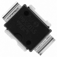
... PD55015STR-E May 2010 RF POWER transistor, LdmoST plastic family Figure 1. Gate Package PowerSO-10RF (formed lead) PowerSO-10RF (straight lead) PowerSO-10RF (formed lead) PowerSO-10RF (straight lead) Doc ID 12596 Rev 2 PD55015-E PD55015S-E PowerSO-10RF (formed lead) PowerSO-10RF (straight lead) Pin connection Source Drain Packing Tube Tube ...
Page 2
... Thermal data . . . . . . . . . . . . . . . . . . . . . . . . . . . . . . . . . . . . . . . . . . . . . . . 3 2 Electrical characteristics . . . . . . . . . . . . . . . . . . . . . . . . . . . . . . . . . . . . . 4 2.1 Static . . . . . . . . . . . . . . . . . . . . . . . . . . . . . . . . . . . . . . . . . . . . . . . . . . . . . 4 2.2 Dynamic . . . . . . . . . . . . . . . . . . . . . . . . . . . . . . . . . . . . . . . . . . . . . . . . . . . 4 2.3 Moisture sensitivity level . . . . . . . . . . . . . . . . . . . . . . . . . . . . . . . . . . . . . . . 4 3 Impedance . . . . . . . . . . . . . . . . . . . . . . . . . . . . . . . . . . . . . . . . . . . . . . . . . 5 4 Typical performance . . . . . . . . . . . . . . . . . . . . . . . . . . . . . . . . . . . . . . . . . 6 4.1 PD55015 4.2 PD55015S Test circuit . . . . . . . . . . . . . . . . . . . . . . . . . . . . . . . . . . . . . . . . . . . . . . . . 11 6 Circuit layout . . . . . . . . . . . . . . . . . . . . . . . . . . . . . . . . . . . . . . . . . . . . . . 12 7 Common source s-parameter . . . . . . . . . . . . . . . . . . . . . . . . . . . . . . . . 13 8 Package mechanical data . . . . . . . . . . . . . . . . . . . . . . . . . . . . . . . . . . . . 19 9 Revision history . . . . . . . . . . . . . . . . . . . . . . . . . . . . . . . . . . . . . . . . . . . 24 2/25 Doc ID 12596 Rev 2 ...
Page 3
... PD55015-E, PD55015S-E 1 Electrical data 1.1 Maximum ratings Table 2. Absolute maximum ratings (T Symbol V (BR)DSS DISS STG 1.2 Thermal data Table 3. Thermal data Symbol R thJC CASE Parameter Drain-source voltage Gate-source voltage Drain current Power dissipation (@ T = 70°C) C Max. operating junction temperature Storage temperature ...
Page 4
... MHz DS Test conditions = 150 500 MHz DQ = 150 mA 500 MHz DQ OUT = 150 mA 500 MHz DQ OUT = 150 mA 500 MHz DQ OUT Test methodology J-STD-020B Doc ID 12596 Rev 2 PD55015-E, PD55015S-E Min Typ Max Unit 1 µA 1 µA 2.0 5.0 V 0.8 V 2.0 2.5 mho 6.5 pF Min ...
Page 5
... PD55015-E, PD55015S-E 3 Impedance Figure 2. Current conventions Table 7. Impedance data Freq. (MHz) 480 1. 0.56 500 1. 0.77 520 1. 1.17 PD55015 Z (Ω) Z (Ω) Freq. (MHz 1. 1.36 1. 1.81 1. 2.13 Doc ID 12596 Rev 2 Impedance PD55015S Z (Ω 480 1. 0.54 1. 0.04 500 1. 0.30 1. 0.22 520 1. 0.11 1. 0.22 876 ...
Page 6
... Figure 3. Capacitance vs. drain voltage C (pF) 1000 100 VDS (V) Figure 5. Gate-source voltage vs. case temperature 1.04 1. 0.96 - Tc, CASE TEMPERATURE (°C) 6/25 Figure 1 Doc ID 12596 Rev 2 PD55015-E, PD55015S-E Drain current vs. gate voltage 3.5 4 4.5 Vgs, GATE-SOURCE VOLTAGE (V) 5 ...
Page 7
... PD55015-E, PD55015S-E 4.1 PD55015-E Figure 6. Output power vs. input power 18 16 480 MHz 14 12 500 MHz 0.2 0.4 Pin, INPUT POWER (W) Figure 8. Drain efficiency vs. output power Pout, OUTPUT POWER (W) Figure 7. 18 520 MHz 12.. 150 0.6 0 Figure 9. 0 480 MHz 520 MHz -10 500 MHz ...
Page 8
... Idq = 150mA Pin = . 520 MHz 500 MHz Pin = . 2.5 3 3.5 Doc ID 12596 Rev 2 PD55015-E, PD55015S-E 480 MHz 520 MHz 500 MHz Pin = .7 W Vdd = 12.5 V 200 400 600 800 Idq, BIAS CURRENT (mA) 480 MHz 500 MHz 520 MHz I = 150mA DQ Pin = . ...
Page 9
... PD55015-E, PD55015S-E 4.2 PD55015S-E Figure 15. Output power vs. input power 18 16 480 MHz 14 12 500 MHz 0.1 0.2 0.3 0.4 Pin, INPUT POWER (W) Figure 17. Drain efficiency vs. output power 60 50 520 MHz Pout, OUTPUT POWER (W) Figure 19. Output power vs. gate bias current Figure 20. Drain efficiency vs. bias current ...
Page 10
... Figure 26. Input return Loss vs. output power Rl (dB) 0 915 MHz 900 MHz 900 MHz -10 876 MHz 876 MHz -20 -30 Vdd = 12.5V Idq = 150mA Doc ID 12596 Rev 2 PD55015-E, PD55015S-E 480 MHz 500 MHz 520 MHz VDS, DRAIN-SOURCE VOLTAGE (V) 915 MHz Pout (W) 915 MHz ...
Page 11
... PD55015-E, PD55015S-E 5 Test circuit Figure 27. Test circuit schematic Table 8. Test circuit component part list Component B1,B2 C1,C12 C2,C3,C4,C11,C12,C13 C6, C18 C9, C15 C8, C16 C7, C17 C5, C10 L1 N1 Z4, Board Ferrite bead - Fair-rite Corp #2743021447 300 pF, 100 mil chip capacitor trimmer capacitor 120 pF 100 mil chip capacitor 10 µ ...
Page 12
... Circuit layout 6 Circuit layout Figure 28. Test fixture component layout Figure 29. Test circuit photomaster 12/25 Doc ID 12596 Rev 2 PD55015-E, PD55015S-E ...
Page 13
... PD55015-E, PD55015S-E 7 Common source s-parameter Table 9. S-parameter for PD55015-E (V Freq < Φ (MHz) 50 0.783 -164 100 0.831 -170 150 0.857 -173 200 0.873 -174 250 0.886 -175 300 0.899 -176 350 0.909 -177 400 0.921 -178 450 0.928 -179 500 0.937 -180 550 0 ...
Page 14
... Common source s-parameter Table 10. S-parameter for PD55015-E (V Freq < Φ (MHz) 50 0.837 -171 100 0.882 -174 150 0.904 -177 200 0.913 -178 250 0.915 -179 300 0.919 -173 350 0.924 179 400 0.928 179 450 0.931 178 500 0.934 178 550 0.938 ...
Page 15
... PD55015-E, PD55015S-E Table 11. S-parameter for PD55015-E (V Freq < Φ (MHz) 50 0.845 -172 100 0.891 -175 150 0.913 -177 200 0.923 -179 250 0.924 -180 300 0.927 180 350 0.930 179 400 0.933 178 450 0.935 178 500 0.938 177 550 0.940 176 600 0 ...
Page 16
... Doc ID 12596 Rev 2 PD55015-E, PD55015S-E < Φ < Φ 0.730 -160 -14 0.746 -166 -21 0.769 -167 -29 0.798 -168 -34 0.851 -168 -39 0.849 -169 -43 0.872 -171 -47 0 ...
Page 17
... PD55015-E, PD55015S-E Table 13. S-parameter PD55015S-E (V Freq < Φ (MHz) 50 0.826 -170 100 0.872 -173 150 0.893 -175 200 0.905 -176 250 0.907 -177 300 0.914 -178 350 0.920 -178 400 0.925 -178 450 0.931 -179 500 0.937 -179 550 0.940 -180 600 ...
Page 18
... Doc ID 12596 Rev 2 PD55015-E, PD55015S-E < Φ < Φ 0.837 -173 -7 0.839 -175 -7 0.841 -176 -11 0.849 -176 -13 0.853 -177 -17 0.861 -177 -17 0.871 -177 -21 0 ...
Page 19
... PD55015-E, PD55015S-E 8 Package mechanical data In order to meet environmental requirements, ST offers these devices in different grades of ® ECOPACK packages, depending on their level of environmental compliance. ECOPACK specifications, grade definitions and product status are available at: www.st.com. ® ECOPACK trademark. Doc ID 12596 Rev 2 Package mechanical data ® ...
Page 20
... Doc ID 12596 Rev 2 PD55015-E, PD55015S-E Inch Min. Typ. Max. 0. 0.0019 0.0038 0.134 0.137 0.142 0.046 0.05 0.054 0.005 0.007 0.009 0.007 0.212 0.217 ...
Page 21
... PD55015-E, PD55015S-E Table 16. PowerSO-10RF straight lead mechanical data Dim Note: Resin protrusions not included (max value: 0.15 mm per side) Figure 31. Package dimensions mm. Min. Typ. Max. 1.62 1.67 1.72 3.4 3.5 3.6 1.2 1.3 1.4 0.15 0.2 0.25 0.2 5.4 5.53 5.65 ...
Page 22
... Package mechanical data Figure 32. Tube information 22/25 Doc ID 12596 Rev 2 PD55015-E, PD55015S-E ...
Page 23
... PD55015-E, PD55015S-E Figure 33. Reel information Doc ID 12596 Rev 2 Package mechanical data 23/25 ...
Page 24
... Revision history 9 Revision history Table 17. Document revision history Date 03-Aug-2006 26-May-2010 24/25 Revision 1 Initial release. 2 Added: Table 6: Moisture sensitivity Doc ID 12596 Rev 2 PD55015-E, PD55015S-E Changes level. ...
Page 25
... PD55015-E, PD55015S-E Information in this document is provided solely in connection with ST products. STMicroelectronics NV and its subsidiaries (“ST”) reserve the right to make changes, corrections, modifications or improvements, to this document, and the products and services described herein at any time, without notice. All ST products are sold pursuant to ST’s terms and conditions of sale. ...