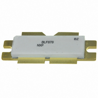
BLF878,112 NXP Semiconductors, BLF878,112 Datasheet - Page 3

BLF878,112
Manufacturer Part Number
BLF878,112
Description
TRANSISTOR RF LDMOS SOT979A
Manufacturer
NXP Semiconductors
Datasheet
1.BLF878112.pdf
(18 pages)
Specifications of BLF878,112
Package / Case
SOT979A
Transistor Type
LDMOS
Frequency
860MHz
Gain
18dB
Voltage - Rated
89V
Current Rating
1.4µA
Current - Test
1.4A
Voltage - Test
40V
Power - Output
300W
Configuration
Dual Common Source
Transistor Polarity
N-Channel
Resistance Drain-source Rds (on)
0.11 Ohms
Drain-source Breakdown Voltage
89 V
Gate-source Breakdown Voltage
13 V
Maximum Operating Temperature
+ 200 C
Mounting Style
SMD/SMT
Minimum Operating Temperature
- 65 C
Application
UHF
Channel Type
N
Channel Mode
Enhancement
Drain Source Voltage (max)
89V
Output Power (max)
300W(Typ)
Power Gain (typ)@vds
21@42VdB
Frequency (min)
470MHz
Frequency (max)
860MHz
Package Type
LDMOST
Pin Count
5
Forward Transconductance (typ)
15.5S
Drain Source Resistance (max)
110(Typ)@6.15Vmohm
Input Capacitance (typ)@vds
190@40VpF
Output Capacitance (typ)@vds
60@40VpF
Reverse Capacitance (typ)
2@40VpF
Operating Temp Range
-65C to 200C
Drain Efficiency (typ)
60%
Mounting
Screw
Mode Of Operation
2-Tone Class-AB/CW Class-AB/DVB-T/PAL BG
Number Of Elements
2
Vswr (max)
10
Screening Level
Military
Lead Free Status / RoHS Status
Lead free / RoHS Compliant
Noise Figure
-
Lead Free Status / Rohs Status
Compliant
Other names
568-4738
934061788112
BLF878
BLF878,112
BLF878
934061788112
BLF878
BLF878,112
BLF878
NXP Semiconductors
4. Limiting values
5. Thermal characteristics
6. Characteristics
BLF878_2
Product data sheet
Table 4.
In accordance with the Absolute Maximum Rating System (IEC 60134).
Table 5.
[1]
[2]
Table 6.
T
[1]
[2]
Symbol
V
V
T
T
Symbol
R
R
Symbol Parameter
V
V
I
I
I
g
R
C
C
C
DSS
DSX
GSS
j
fs
stg
j
DS
GS
(BR)DSS
GS(th)
th(j-c)
th(c-h)
DS(on)
iss
oss
rss
= 25 C unless otherwise specified.
R
R
I
Capacitance values without internal matching.
D
th(j-c)
th(c-h)
is the drain current.
is measured under RF conditions.
drain-source breakdown voltage V
gate-source threshold voltage
drain leakage current
drain cut-off current
gate leakage current
forward transconductance
drain-source on-state resistance V
input capacitance
output capacitance
reverse transfer capacitance
is dependent on the applied thermal compound and clamping/mounting of the device.
Limiting values
Thermal characteristics
Characteristics
Parameter
thermal resistance from junction to case
thermal resistance from case to heatsink
Parameter
drain-source voltage
gate-source voltage
storage temperature
junction temperature
Rev. 02 — 15 June 2009
Conditions
V
V
V
V
V
V
I
V
f = 1 MHz
V
f = 1 MHz
V
f = 1 MHz
D
GS
DS
GS
GS
DS
GS
DS
GS
GS
GS
GS
= 7.6 A
Conditions
= 10 V; I
= 10 V
= 10 V; I
= 0 V; I
= 0 V; V
= V
= 11 V; V
= V
= 0 V; V
= 0 V; V
= 0 V; V
GSth
GSth
D
DS
+ 3.75 V;
+ 3.75 V;
DS
DS
DS
D
D
= 2.25 mA
DS
= 225 mA
= 11.2 A
= 42 V
= 40 V;
= 40 V;
= 40 V;
= 0 V
Conditions
T
P
UHF power LDMOS transistor
case
L(AV)
= 80 C;
= 150 W
[1]
[1]
[1]
[1]
[2]
[2]
[2]
Min
-
-
0.5
65
Min Typ Max
89
1.4
-
35
-
-
-
-
-
-
© NXP B.V. 2009. All rights reserved.
-
1.9
-
39
-
15.5 -
110 -
190 -
60
2
Max
89
+11
+150
200
BLF878
[1]
[2]
Typ
0.23
0.15
105.5 V
2.4
1.4
-
140
-
-
Unit
V
V
C
C
3 of 18
Unit
K/W
K/W
Unit
V
A
nA
S
m
pF
pF
pF
A


