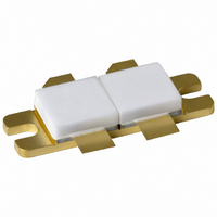
BLF248,112 NXP Semiconductors, BLF248,112 Datasheet - Page 6

BLF248,112
Manufacturer Part Number
BLF248,112
Description
TRANSISTOR RF DMOS SOT262A1
Manufacturer
NXP Semiconductors
Datasheet
1.BLF248112.pdf
(16 pages)
Specifications of BLF248,112
Package / Case
SOT-262A1
Transistor Type
2 N-Channel (Dual)
Frequency
225MHz
Gain
11.5dB
Voltage - Rated
65V
Current Rating
25A
Voltage - Test
28V
Power - Output
300W
Minimum Operating Temperature
- 65 C
Mounting Style
SMD/SMT
Product Type
RF MOSFET Power
Resistance Drain-source Rds (on)
0.15 Ohms
Transistor Polarity
N-Channel
Configuration
Dual Common Source
Drain-source Breakdown Voltage
65 V
Gate-source Breakdown Voltage
+/- 20 V
Continuous Drain Current
25 A
Power Dissipation
500 W
Maximum Operating Temperature
+ 150 C
Lead Free Status / RoHS Status
Lead free / RoHS Compliant
Noise Figure
-
Current - Test
-
Lead Free Status / RoHS Status
Lead free / RoHS Compliant, Lead free / RoHS Compliant
Other names
568-2389
934006630112
BLF248
BLF248
934006630112
BLF248
BLF248
Philips Semiconductors
APPLICATION INFORMATION FOR CLASS-AB OPERATION
T
RF performance in a linear amplifier in a common source class-AB circuit.
R
Ruggedness in class-AB operation
The BLF248 is capable of withstanding a load mismatch corresponding to VSWR = 50 through all phases under the
following conditions:
V
2003 Sep 02
handbook, halfpage
class-AB
h
DS
GS
VHF push-pull power MOS transistor
= 25 C; R
V
Fig.8
GS
= 28 V; f = 225 MHz at rated output power.
(pF)
= 536
C rs
600
400
200
= 0; f = 1 MHz.
MODE OF OPERATION
0
0
Feedback capacitance as a function of
drain-source voltage; typical values per
section.
th mb-h
per section; optimum load impedance per section = 0.79
10
= 0.15 K/W, unless otherwise specified.
20
30
V DS (V)
MGP208
(MHz)
225
175
f
40
6
V
(V)
28
28
DS
j0.11 .
300
300
(W)
P
L
typ. 11.5
typ. 13
(dB)
G
10
p
Product specification
BLF248
typ. 65
typ. 67
(%)
55
D


