BLF861A,112 NXP Semiconductors, BLF861A,112 Datasheet - Page 2
BLF861A,112
Manufacturer Part Number
BLF861A,112
Description
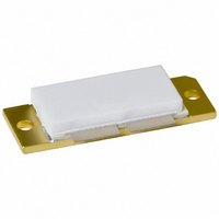
TRANSISTOR RF LDMOS SOT540A
Manufacturer
NXP Semiconductors
Datasheet
1.BLF861A112.pdf
(16 pages)
Specifications of BLF861A,112
Package / Case
SOT540A
Transistor Type
LDMOS
Frequency
860MHz
Gain
14.5dB
Voltage - Rated
65V
Current Rating
18A
Current - Test
1A
Voltage - Test
32V
Power - Output
150W
Minimum Operating Temperature
- 65 C
Mounting Style
SMD/SMT
Resistance Drain-source Rds (on)
0.16 Ohm (Typ)
Transistor Polarity
N-Channel
Configuration
Single Dual Drain Dual Gate
Drain-source Breakdown Voltage
65 V
Gate-source Breakdown Voltage
+/- 15 V
Continuous Drain Current
18 A
Power Dissipation
318000 mW
Maximum Operating Temperature
+ 200 C
Application
UHF
Channel Type
N
Channel Mode
Enhancement
Drain Source Voltage (max)
65V
Output Power (max)
150W
Power Gain (typ)@vds
14.5@32V/14(Min)@32VdB
Frequency (max)
860MHz
Package Type
LDMOST
Pin Count
5
Forward Transconductance (typ)
4S
Drain Source Resistance (max)
160(Typ)mohm
Input Capacitance (typ)@vds
82@32VpF
Output Capacitance (typ)@vds
40@32VpF
Reverse Capacitance (typ)
6@32VpF
Operating Temp Range
-65C to 200C
Drain Efficiency (typ)
50%
Mounting
Screw
Mode Of Operation
2-Tone Class-AB/CW Class-AB/PAL BG Class-AB
Number Of Elements
1
Power Dissipation (max)
318000mW
Vswr (max)
10
Screening Level
Military
Lead Free Status / RoHS Status
Lead free / RoHS Compliant
Noise Figure
-
Lead Free Status / Rohs Status
Lead free / RoHS Compliant
Other names
568-2407
934056499112
BLF861A
BLF861A
934056499112
BLF861A
BLF861A
Available stocks
Company
Part Number
Manufacturer
Quantity
Price

Part Number:
BLF861A,112
Manufacturer:
NXP/恩智浦
Quantity:
20 000


Philips Semiconductors
FEATURES
APPLICATIONS
DESCRIPTION
Silicon N-channel enhancement mode lateral D-MOS
push-pull transistor in a SOT540A package with ceramic
cap. The common source is connected to the mounting
flange.
QUICK REFERENCE DATA
RF performance at T
Note
1. Sync compression: input sync
LIMITING VALUES
In accordance with the Absolute Maximum Rating System (IEC 60134).
2001 Feb 09
CW, class-AB
PAL BG (TV); class-AB
V
V
I
P
T
T
D
SYMBOL
stg
j
High power gain
Easy power control
Excellent ruggedness
Designed to withstand abrupt load mismatch errors
Source on underside eliminates DC isolators; reducing
common mode inductance
Designed for broadband operation (UHF band)
Internal input and output matching for high gain and
optimum broadband operation.
Communication transmitter applications in the UHF
frequency range.
DS
GS
tot
UHF power LDMOS transistor
MODE OF OPERATION
drain-source voltage
gate-source voltage
drain current (DC)
total power dissipation
storage temperature
junction temperature
h
= 25 C in a common source 860 MHz test circuit.
PARAMETER
860 (ch 69)
33%; output sync 27%.
(MHz)
860
f
T
V
mb
(V)
32
32
DS
CONDITIONS
25 C
2
PINNING - SOT540A
(peak sync)
typ. 170
>150
150
(W)
PIN
P
1
2
3
4
5
L
Top view
Fig.1 Simplified outline.
65
typ. 14.5
drain 1
drain 2
gate 1
gate 2
source connected to flange
>13.5
MIN.
(dB)
>14
G
p
3
1
DESCRIPTION
65
18
318
+150
200
15
2
4
MAX.
>50
>40
Product specification
(%)
MBK777
D
5
BLF861A
V
V
A
W
C
C
note 1
UNIT
(dB)
G
1
p
Related parts for BLF861A,112
Image
Part Number
Description
Manufacturer
Datasheet
Request
R

Part Number:
Description:
Silicon N-channel enhancement mode lateral D-MOS push-pull transistor in a SOT540A package with ceramic cap
Manufacturer:
NXP Semiconductors
Datasheet:

Part Number:
Description:
Uhf Power Ldmos Transistor
Manufacturer:
NXP Semiconductors
Datasheet:
Part Number:
Description:
NXP Semiconductors designed the LPC2420/2460 microcontroller around a 16-bit/32-bitARM7TDMI-S CPU core with real-time debug interfaces that include both JTAG andembedded trace
Manufacturer:
NXP Semiconductors
Datasheet:

Part Number:
Description:
NXP Semiconductors designed the LPC2458 microcontroller around a 16-bit/32-bitARM7TDMI-S CPU core with real-time debug interfaces that include both JTAG andembedded trace
Manufacturer:
NXP Semiconductors
Datasheet:
Part Number:
Description:
NXP Semiconductors designed the LPC2468 microcontroller around a 16-bit/32-bitARM7TDMI-S CPU core with real-time debug interfaces that include both JTAG andembedded trace
Manufacturer:
NXP Semiconductors
Datasheet:
Part Number:
Description:
NXP Semiconductors designed the LPC2470 microcontroller, powered by theARM7TDMI-S core, to be a highly integrated microcontroller for a wide range ofapplications that require advanced communications and high quality graphic displays
Manufacturer:
NXP Semiconductors
Datasheet:
Part Number:
Description:
NXP Semiconductors designed the LPC2478 microcontroller, powered by theARM7TDMI-S core, to be a highly integrated microcontroller for a wide range ofapplications that require advanced communications and high quality graphic displays
Manufacturer:
NXP Semiconductors
Datasheet:
Part Number:
Description:
The Philips Semiconductors XA (eXtended Architecture) family of 16-bit single-chip microcontrollers is powerful enough to easily handle the requirements of high performance embedded applications, yet inexpensive enough to compete in the market for hi
Manufacturer:
NXP Semiconductors
Datasheet:
Part Number:
Description:
The XA-S3 device is a member of Philips Semiconductors? XA(eXtended Architecture) family of high performance 16-bitsingle-chip microcontrollers
Manufacturer:
NXP Semiconductors
Datasheet:

Part Number:
Description:
The NXP BlueStreak LH75401/LH75411 family consists of two low-cost 16/32-bit System-on-Chip (SoC) devices
Manufacturer:
NXP Semiconductors
Datasheet:
Part Number:
Description:
The NXP LPC3130/3131 combine an 180 MHz ARM926EJ-S CPU core, high-speed USB2
Manufacturer:
NXP Semiconductors
Datasheet:
Part Number:
Description:
The NXP LPC3141 combine a 270 MHz ARM926EJ-S CPU core, High-speed USB 2
Manufacturer:
NXP Semiconductors
Part Number:
Description:
The NXP LPC3143 combine a 270 MHz ARM926EJ-S CPU core, High-speed USB 2
Manufacturer:
NXP Semiconductors

Part Number:
Description:
The NXP LPC3152 combines an 180 MHz ARM926EJ-S CPU core, High-speed USB 2
Manufacturer:
NXP Semiconductors