NTD50N03R-035 ON Semiconductor, NTD50N03R-035 Datasheet - Page 2
NTD50N03R-035
Manufacturer Part Number
NTD50N03R-035
Description
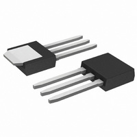
MOSFET N-CH 25V 7.8A IPAK
Manufacturer
ON Semiconductor
Datasheet
1.NTD50N03R.pdf
(8 pages)
Specifications of NTD50N03R-035
Fet Type
MOSFET N-Channel, Metal Oxide
Fet Feature
Logic Level Gate
Rds On (max) @ Id, Vgs
12 mOhm @ 30A, 11.5V
Drain To Source Voltage (vdss)
25V
Current - Continuous Drain (id) @ 25° C
7.8A
Vgs(th) (max) @ Id
2V @ 250µA
Gate Charge (qg) @ Vgs
15nC @ 11.5V
Input Capacitance (ciss) @ Vds
750pF @ 12V
Power - Max
1.5W
Mounting Type
Through Hole
Package / Case
IPak, TO-251, DPak (3 straight short leads + tab)
Lead Free Status / RoHS Status
Contains lead / RoHS non-compliant


3. Surface−mounted on FR4 board using 1 sq in pad, 1 oz Cu.
4. Surface−mounted on FR4 board using the minimum recommended pad size.
5. Pulse Test: Pulse Width ≤ 300 ms, Duty Cycle ≤ 2%.
OFF CHARACTERISTICS
ON CHARACTERISTICS (Note 5)
CHARGES, CAPACITANCES AND GATE RESISTANCE
THERMAL RESISTANCE MAXIMUM RATINGS
ELECTRICAL CHARACTERISTICS
Junction−to−Case (Drain)
Junction−to−Ambient − Steady State (Note 3)
Junction−to−Ambient − Steady State (Note 4)
Drain−to−Source Breakdown Voltage
Drain−to−Source Breakdown Voltage
Zero Gate Voltage Drain Current
Gate−to−Source Leakage Current
Gate Threshold Voltage
Negative Threshold Temperature Coefficient
Drain−to−Source On Resistance
Forward Transconductance
Input Capacitance
Output Capacitance
Reverse Transfer Capacitance
Total Gate Charge
Threshold Gate Charge
Gate−to−Source Charge
Gate−to−Drain Charge
Total Gate Charge
Threshold Gate Charge
Gate−to−Source Charge
Gate−to−Drain Charge
Temperature Coefficient
Parameter
Parameter
(T
J
= 25°C unless otherwise noted)
V
V
V
(BR)DSS
Symbol
Q
Q
V
GS(TH)
R
Q
Q
(BR)DSS
GS(TH)
I
I
C
G(TOT)
Q
Q
G(TOT)
Q
Q
DS(on)
C
C
g
GSS
G(TH)
G(TH)
DSS
oss
FS
rss
GS
GD
GS
GD
iss
/T
/T
http://onsemi.com
J
J
NTD50N03R
V
V
V
V
V
V
V
V
GS
V
V
GS
V
GS
GS
DS
GS
DS
GS
V
GS
GS
GS
DS
2
= 11.5 V
= 4.5 V
= 11.5 V, V
= 20 V
= 10 V
Test Condition
= 0 V,
= 0 V, V
= 4.5 V, V
= V
= 0 V, f = 1.0 MHz,
= 0 V, I
= 15 V, I
V
I
I
DS
D
D
DS
= 30 A
= 30 A
, I
= 12 V
GS
D
D
D
DS
= 250 mA
T
= 250 mA
DS
T
= "20 V
I
I
I
I
I
J
= 15 A
D
D
D
D
D
J
= 15 V,
= 125°C
= 15 V,
= 25°C
= 30 A
= 15 A
= 30 A
= 30 A
= 15 A
Symbol
R
R
R
qJC
qJA
qJA
Min
1.0
25
−5.0
12.5
11.7
Typ
−16
610
300
125
1.7
6.0
0.9
1.9
3.7
1.0
1.9
3.9
12
21
19
15
15
Value
71.4
100
3.0
"100
Max
750
1.5
2.0
10
14
23
10
mV/°C
mV/°C
°C/W
Unit
Unit
mW
nA
nC
nC
mA
pF
V
V
S
Related parts for NTD50N03R-035
Image
Part Number
Description
Manufacturer
Datasheet
Request
R

Part Number:
Description:
ON Semiconductor [VOLTAGE REGULATOR]
Manufacturer:
ON Semiconductor
Datasheet:
Part Number:
Description:
357-036-542-201 CARDEDGE 36POS DL .156 BLK LOPRO
Manufacturer:
ON Semiconductor
Datasheet:
Part Number:
Description:
357-036-542-201 CARDEDGE 36POS DL .156 BLK LOPRO
Manufacturer:
ON Semiconductor
Datasheet:
Part Number:
Description:
357-036-542-201 CARDEDGE 36POS DL .156 BLK LOPRO
Manufacturer:
ON Semiconductor
Datasheet:
Part Number:
Description:
357-036-542-201 CARDEDGE 36POS DL .156 BLK LOPRO
Manufacturer:
ON Semiconductor
Datasheet:
Part Number:
Description:
357-036-542-201 CARDEDGE 36POS DL .156 BLK LOPRO
Manufacturer:
ON Semiconductor
Datasheet:
Part Number:
Description:
357-036-542-201 CARDEDGE 36POS DL .156 BLK LOPRO
Manufacturer:
ON Semiconductor
Datasheet:
Part Number:
Description:
357-036-542-201 CARDEDGE 36POS DL .156 BLK LOPRO
Manufacturer:
ON Semiconductor
Datasheet:
Part Number:
Description:
357-036-542-201 CARDEDGE 36POS DL .156 BLK LOPRO
Manufacturer:
ON Semiconductor
Datasheet:
Part Number:
Description:
357-036-542-201 CARDEDGE 36POS DL .156 BLK LOPRO
Manufacturer:
ON Semiconductor
Datasheet:
Part Number:
Description:
357-036-542-201 CARDEDGE 36POS DL .156 BLK LOPRO
Manufacturer:
ON Semiconductor
Datasheet:
Part Number:
Description:
Manufacturer:
ON Semiconductor
Datasheet:
Part Number:
Description:
Manufacturer:
ON Semiconductor
Datasheet:
Part Number:
Description:
Manufacturer:
ON Semiconductor
Datasheet: