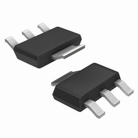
NTF3055-160T1 ON Semiconductor, NTF3055-160T1 Datasheet - Page 4

NTF3055-160T1
Manufacturer Part Number
NTF3055-160T1
Description
MOSFET N-CH 60V 2A SOT223
Manufacturer
ON Semiconductor
Datasheet
1.NTF3055-160T3LF.pdf
(8 pages)
Specifications of NTF3055-160T1
Fet Type
MOSFET N-Channel, Metal Oxide
Fet Feature
Standard
Rds On (max) @ Id, Vgs
160 mOhm @ 1A, 10V
Drain To Source Voltage (vdss)
60V
Current - Continuous Drain (id) @ 25° C
2A
Vgs(th) (max) @ Id
4V @ 250µA
Gate Charge (qg) @ Vgs
14nC @ 10V
Input Capacitance (ciss) @ Vds
280pF @ 25V
Power - Max
1.3W
Mounting Type
Surface Mount
Package / Case
SOT-223 (3 leads + Tab), SC-73, TO-261
Lead Free Status / RoHS Status
Contains lead / RoHS non-compliant
Other names
NTF3055-160T1OS
0.001
0.01
560
480
400
320
240
160
100
100
0.1
80
10
10
0
1
1
10
0.1
1
GATE–TO–SOURCE OR DRAIN–TO–SOURCE VOLTAGE
V GS = 20 V
SINGLE PULSE
T C = 25 C
C iss
C rss
V DS = 30 V
I D = 2 A
V GS = 10 V
Figure 9. Resistive Switching Time Variation
V DS = 0 V
Figure 11. Maximum Rated Forward Biased
V DS , DRAIN–TO–SOURCE VOLTAGE (VOLTS)
t d(on)
t d(off)
5
dc
V GS
Figure 7. Capacitance Variation
t r
THERMAL LIMIT
PACKAGE LIMIT
R DS(on) LIMIT
R G , GATE RESISTANCE ( )
versus Gate Resistance
t f
10 ms
0
Safe Operating Area
V DS
1
V GS = 0 V
1 ms
5
(VOLTS)
10
10
100 s
C oss
C iss
C rss
10
15
10 s
T J = 25 C
20
http://onsemi.com
NTF3055–160
100
100
25
4
1.6
1.2
0.8
0.4
12
10
70
60
50
40
30
20
10
8
6
4
2
0
2
0
0
0.6
0
Figure 10. Diode Forward Voltage versus Current
25
Figure 12. Maximum Avalanche Energy versus
Drain–to–Source Voltage versus Total Charge
V GS = 0 V
T J = 25 C
Q 1
V SD , SOURCE–TO–DRAIN VOLTAGE (VOLTS)
T J , STARTING JUNCTION TEMPERATURE ( C)
0.64
1
50
Starting Junction Temperature
Figure 8. Gate–to–Source and
Q g , TOTAL GATE CHARGE (nC)
2
0.68
75
Q 2
3
0.72
Q T
100
4
0.76
V GS
5
125
0.8
6
I D = 6 A
I D = 2 A
T J = 25 C
150
0.84
7
0.88
175
8


