NTF3055-160T1 ON Semiconductor, NTF3055-160T1 Datasheet

MOSFET N-CH 60V 2A SOT223

NTF3055-160T1

Manufacturer Part Number
NTF3055-160T1
Description
MOSFET N-CH 60V 2A SOT223
Manufacturer
ON Semiconductor
Datasheet

Specifications of NTF3055-160T1

Fet Type
MOSFET N-Channel, Metal Oxide
Fet Feature
Standard
Rds On (max) @ Id, Vgs
160 mOhm @ 1A, 10V
Drain To Source Voltage (vdss)
60V
Current - Continuous Drain (id) @ 25° C
2A
Vgs(th) (max) @ Id
4V @ 250µA
Gate Charge (qg) @ Vgs
14nC @ 10V
Input Capacitance (ciss) @ Vds
280pF @ 25V
Power - Max
1.3W
Mounting Type
Surface Mount
Package / Case
SOT-223 (3 leads + Tab), SC-73, TO-261
Lead Free Status / RoHS Status
Contains lead / RoHS non-compliant
Other names
NTF3055-160T1OS
N–Channel SOT–223
power supplies, converters and power motor controls and bridge
circuits.
Applications
1. When surface mounted to an FR4 board using 1 pad size,
2. When surface mounted to an FR4 board using minimum recommended pad
July, 2001 – Rev. 0
MAXIMUM RATINGS
Drain–to–Source Voltage
Drain–to–Gate Voltage (R GS = 1.0 M )
Gate–to–Source Voltage
Drain Current
Total Power Dissipation @ T A = 25 C (Note 1.)
Total Power Dissipation @ T A = 25 C (Note 2.)
Operating and Storage Temperature Range
Single Pulse Drain–to–Source Avalanche
Thermal Resistance
Maximum Lead Temperature for Soldering
Designed for low voltage, high speed switching applications in
Power Supplies
Converters
Power Motor Controls
Bridge Circuits
Semiconductor Components Industries, LLC, 2001
(Cu. Area 1.127 in 2 ).
size, 2–2.4 oz. (Cu. Area 0.272 in 2 ).
– Continuous @ T A = 25 C
– Continuous @ T A = 100 C
– Single Pulse (t p
Derate above 25 C
Energy – Starting T J = 25 C
(V DD = 25 Vdc, V GS = 10 Vdc,
I L (pk) = 6.0 Apk, L = 10 mH, V DS = 60 Vdc)
Purposes, 1/8 from case for 10 seconds
– Continuous
– Non–repetitive (t p
– Junction to Ambient (Note 1.)
– Junction to Ambient (Note 2.)
Rating
10 s)
(T C = 25 C unless otherwise noted)
10 ms)
Preferred Device
Symbol
T J , T stg
V DGR
V DSS
R JA
R JA
V GS
E AS
I DM
P D
T L
I D
I D
–55 to
Value
0.014
72.3
175
260
114
2.0
1.2
6.0
2.1
1.3
60
60
65
20
30
1
W/ C
Unit
Vdc
Vdc
Vdc
Vpk
Adc
Apk
C/W
mJ
W
W
C
C
NTF3055–160T1
NTF3055–160T3
NTF3055–160T3LF
1
2
Device
3
ORDERING INFORMATION
R DS(on) = 160 mW
5160
L
WW
4
http://onsemi.com
PIN ASSIGNMENT
2.0 AMPERES
60 VOLTS
CASE 318E
1
SOT–223
STYLE 3
SOT–223 1000 Tape & Reel
SOT–223 4000 Tape & Reel
= Device Code
= Location Code
= Work Week
N–Channel
Package
Publication Order Number:
4
2
3
NTF3055–160/D
Shipping
MARKING
DIAGRAM
LWW
5160

Related parts for NTF3055-160T1

NTF3055-160T1 Summary of contents

Page 1

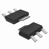
... CASE 318E LWW STYLE 3 5160 = Device Code L = Location Code WW = Work Week PIN ASSIGNMENT ORDERING INFORMATION Package Shipping SOT–223 1000 Tape & Reel SOT–223 4000 Tape & Reel SOT–223 4000 Tape & Reel Publication Order Number: NTF3055–160/D ...

Page 2

... Gate Charge SOURCE–DRAIN DIODE CHARACTERISTICS Forward On–Voltage Reverse Recovery Time Reverse Recovery Stored Charge 3. Pulse Test: Pulse Width 300 s, Duty Cycle 4. Switching characteristics are independent of operating junction temperatures. NTF3055–160 ( unless otherwise noted) Symbol V (BR)DSS I DSS 20 Vdc Vdc) I GSS V GS(th) ...

Page 3

... V GS, GATE–TO–SOURCE VOLTAGE (VOLTS 1.8 1.6 1.4 1.2 1 0.8 0.6 –50 – 100 JUNCTION TEMPERATURE ( C) Figure 5. On–Resistance Variation with Temperature NTF3055–160 2 5.5 V 2 1 100 C 0 2.4 2.8 3 3.4 3.8 V GS, GATE–TO–SOURCE VOLTAGE (VOLTS) Figure 2 ...

Page 4

... Gate Resistance 100 SINGLE PULSE 0 100 s 0.01 R DS(on) LIMIT THERMAL LIMIT PACKAGE LIMIT 0.001 0 DRAIN–TO–SOURCE VOLTAGE (VOLTS) Figure 11. Maximum Rated Forward Biased Safe Operating Area NTF3055–160 Drain–to–Source Voltage versus Total Charge 1.6 1.2 0.8 0.4 ...

Page 5

... D = 0.5 0.2 10 0.1 0.05 1 0.01 SINGLE PULSE 0.1 0.00001 0.0001 0.001 NTF3055–160 0.01 0 TIME (s) Figure 13. Thermal Response http://onsemi.com 5 10 100 1000 ...

Page 6

... NTF3055–160 PACKAGE DIMENSIONS SOT–223 (TO–261) CASE 318E–04 ISSUE http://onsemi.com ...

Page 7

... Notes NTF3055–160 http://onsemi.com 7 ...

Page 8

... NTF3055–160 JAPAN: ON Semiconductor, Japan Customer Focus Center 4–32–1 Nishi–Gotanda, Shinagawa–ku, Tokyo, Japan 141–0031 Phone: 81–3–5740–2700 Email: r14525@onsemi.com ON Semiconductor Website: http://onsemi.com For additional information, please contact your local Sales Representative. http://onsemi.com 8 NTF3055–160/D ...

Related keywords