IRFR3418PBF International Rectifier, IRFR3418PBF Datasheet - Page 2
IRFR3418PBF
Manufacturer Part Number
IRFR3418PBF
Description
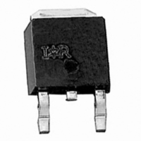
MOSFET N-CH 80V 70A DPAK
Manufacturer
International Rectifier
Series
HEXFET®r
Datasheet
1.IRFU3418PBF.pdf
(11 pages)
Specifications of IRFR3418PBF
Fet Type
MOSFET N-Channel, Metal Oxide
Fet Feature
Standard
Rds On (max) @ Id, Vgs
14 mOhm @ 18A, 10V
Drain To Source Voltage (vdss)
80V
Current - Continuous Drain (id) @ 25° C
70A
Vgs(th) (max) @ Id
5.5V @ 250µA
Gate Charge (qg) @ Vgs
94nC @ 10V
Input Capacitance (ciss) @ Vds
3510pF @ 25V
Power - Max
3.8W
Mounting Type
Surface Mount
Package / Case
DPak, TO-252 (2 leads+tab), SC-63
Lead Free Status / RoHS Status
Lead free / RoHS Compliant
Available stocks
Company
Part Number
Manufacturer
Quantity
Price
Company:

Part Number:
IRFR3418PBF
Manufacturer:
INTERNATIONAL RECTIFIER
Quantity:
30 000


V
∆V
R
V
I
I
gfs
Q
Q
Q
t
t
t
t
C
C
C
C
C
C
E
I
I
I
V
t
Q
t
Static @ T
Dynamic @ T
Avalanche Characteristics
Diode Characteristics
DSS
GSS
d(on)
r
d(off)
f
AR
S
SM
rr
on
(BR)DSS
DS(on)
GS(th)
iss
oss
rss
oss
oss
oss
AS
SD
g
gs
gd
rr
2
(BR)DSS
eff.
/∆T
J
J
Drain-to-Source Breakdown Voltage
Breakdown Voltage Temp. Coefficient
Static Drain-to-Source On-Resistance
Gate Threshold Voltage
Drain-to-Source Leakage Current
Gate-to-Source Forward Leakage
Gate-to-Source Reverse Leakage
Forward Transconductance
Total Gate Charge
Gate-to-Source Charge
Gate-to-Drain ("Miller") Charge
Turn-On Delay Time
Rise Time
Turn-Off Delay Time
Fall Time
Input Capacitance
Output Capacitance
Reverse Transfer Capacitance
Output Capacitance
Output Capacitance
Effective Output Capacitance
Single Pulse Avalanche Energy
Avalanche Current
Continuous Source Current
(Body Diode)
Pulsed Source Current
(Body Diode)
Diode Forward Voltage
Reverse Recovery Time
Reverse Recovery Charge
Forward Turn-On Time
= 25°C (unless otherwise specified)
J
Parameter
= 25°C (unless otherwise specified)
Ùh
Parameter
Parameter
Parameter
Ù
h
Intrinsic turn-on time is negligible (turn-on is dominated by LS+LD)
Min. Typ. Max. Units
Min. Typ. Max. Units
Min. Typ. Max. Units
–––
–––
–––
–––
–––
–––
–––
–––
–––
–––
–––
–––
–––
–––
–––
–––
–––
–––
–––
–––
–––
–––
–––
–––
3.5
80
66
3510
1220
0.08
11.5
–––
–––
–––
–––
–––
–––
–––
330
190
240
360
–––
–––
–––
130
63
23
23
24
72
41
27
57
Typ.
-100
–––
–––
250
100
–––
–––
–––
–––
–––
–––
–––
–––
–––
–––
–––
–––
–––
–––
–––
280
–––
–––
5.5
1.0
1.3
14
94
70
V/°C
mΩ
nC
µA
nA
pF
nC
ns
ns
V
V
S
A
V
V
Reference to 25°C, I
V
V
V
V
V
V
V
I
V
V
V
I
R
V
V
V
ƒ = 1.0MHz
V
V
V
MOSFET symbol
showing the
integral reverse
p-n junction diode.
T
T
di/dt = 100A/µs
D
D
J
J
GS
GS
DS
DS
DS
GS
GS
DS
DS
GS
DD
G
GS
GS
DS
GS
GS
GS
= 18A
= 18A
= 25°C, I
= 150°C, I
= 6.8Ω
= 0V, I
= 10V, I
= V
= 80V, V
= 64V, V
= 20V
= -20V
= 25V, I
= 40V
= 10V
= 40V
= 10V
= 0V
= 25V
= 0V, V
= 0V, V
= 0V, V
GS
Max.
260
, I
18
D
f
f
Conditions
Conditions
Conditions
D
S
DS
D
D
DS
DS
= 250µA
GS
GS
F
= 250µA
= 18A, V
= 18A
= 18A
= 0V to 64V
= 18A, V
= 1.0V, ƒ = 1.0MHz
= 64V, ƒ = 1.0MHz
= 0V
= 0V, T
f
www.irf.com
D
f
= 1mA
G
GS
J
DD
= 150°C
= 0V
= 25V
Units
e
mJ
A
f
S
D
Related parts for IRFR3418PBF
Image
Part Number
Description
Manufacturer
Datasheet
Request
R

Part Number:
Description:
Power MOSFET(Vdss=100V, Rds(on)=0.21ohm, Id=9.4A)
Manufacturer:
IRF [International Rectifier]
Datasheet:
Part Number:
Description:
Advanced Power MOSFET
Manufacturer:
FAIRCHILD [Fairchild Semiconductor]
Datasheet:

Part Number:
Description:
SCHOTTKY RECTIFIER
Manufacturer:
International Rectifier Corp.
Datasheet:
Part Number:
Description:
SCHOTTKY RECTIFIER
Manufacturer:
International Rectifier Corp.
Datasheet:
Part Number:
Description:
SCHOTTKY RECTIFIER
Manufacturer:
International Rectifier Corp.
Datasheet:
Part Number:
Description:
SCHOTTKY RECTIFIER
Manufacturer:
International Rectifier Corp.
Datasheet:
Part Number:
Description:
SCHOTTKY RECTIFIER
Manufacturer:
International Rectifier Corp.
Datasheet:
Part Number:
Description:
SCHOTTKY RECTIFIER
Manufacturer:
International Rectifier Corp.
Datasheet:
Part Number:
Description:
SCHOTTKY RECTIFIER
Manufacturer:
International Rectifier Corp.
Datasheet:
Part Number:
Description:
SCHOTTKY RECTIFIER
Manufacturer:
International Rectifier Corp.
Datasheet:
Part Number:
Description:
SCHOTTKY RECTIFIER
Manufacturer:
International Rectifier Corp.
Datasheet:
Part Number:
Description:
SCHOTTKY RECTIFIER
Manufacturer:
International Rectifier Corp.
Datasheet:
Part Number:
Description:
SCHOTTKY RECTIFIER
Manufacturer:
International Rectifier Corp.
Datasheet:
Part Number:
Description:
SCHOTTKY RECTIFIER
Manufacturer:
International Rectifier Corp.
Datasheet:
Part Number:
Description:
SCHOTTKY RECTIFIER
Manufacturer:
International Rectifier Corp.
Datasheet: