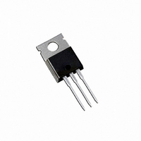
IRF1607 International Rectifier, IRF1607 Datasheet

IRF1607
Specifications of IRF1607
Available stocks
Related parts for IRF1607
IRF1607 Summary of contents
Page 1
... JC R Case-to-Sink, Flat, Greased Surface CS R Junction-to-Ambient JA www.irf.com AUTOMOTIVE MOSFET G Power MOSFETs @ 10V GS @ 10V GS See Fig.12a, 12b, 15, 16 300 (1.6mm from case ) Typ. 0.50 PD -94158 IRF1607 ® HEXFET Power MOSFET 75V DSS R = 0.0075 DS(on 142A D S TO-220AB Max. Units 142 100 ...
Page 2
... IRF1607 Electrical Characteristics @ T Parameter V Drain-to-Source Breakdown Voltage (BR)DSS Breakdown Voltage Temp. Coefficient (BR)DSS J R Static Drain-to-Source On-Resistance DS(on) V Gate Threshold Voltage GS(th) g Forward Transconductance fs I Drain-to-Source Leakage Current DSS Gate-to-Source Forward Leakage I GSS Gate-to-Source Reverse Leakage Q Total Gate Charge g Q Gate-to-Source Charge ...
Page 3
... Fig 2. Typical Output Characteristics 3 2.5 2.0 1.5 1.0 0.5 = 25V 0.0 -60 -40 -20 0 8.0 9.0 10.0 Fig 4. Normalized On-Resistance IRF1607 VGS 15V 10V 8.0V 7.0V 6.0V 5.5V 5.0V 4.5V 4.5V 20µs PULSE WIDTH ° 175 Drain-to-Source Voltage (V) DS ...
Page 4
... IRF1607 12000 0V, C iss = rss = C gd 10000 C oss = Ciss 8000 6000 Coss 4000 2000 Crss Drain-to-Source Voltage (V) Fig 5. Typical Capacitance Vs. Drain-to-Source Voltage 1000 ° 175 C J 100 10 ° 0.1 0.2 0.6 1.0 1.4 V ,Source-to-Drain Voltage (V) SD Fig 7. Typical Source-Drain Diode Forward Voltage ...
Page 5
... Fig 11. Maximum Effective Transient Thermal Impedance, Junction-to-Case www.irf.com R G 10V Pulse Width Duty Factor Fig 10a. Switching Time Test Circuit V DS 90% 150 175 ° 10 d(on) Fig 10b. Switching Time Waveforms Notes: 1. Duty factor Peak 0.001 0. Rectangular Pulse Duration (sec) 1 IRF1607 D.U. µ d(off ...
Page 6
... IRF1607 Fig 12a. Unclamped Inductive Test Circuit Fig 12b. Unclamped Inductive Waveforms Charge Fig 13a. Basic Gate Charge Waveform Current Regulator Same Type as D.U.T. 50K .2 F 12V .3 F D.U. 3mA Current Sampling Resistors Fig 13b. Gate Charge Test Circuit 6 3000 1 5V ...
Page 7
... Figure 15, 16). jmax t Average time in avalanche 125 150 175 D = Duty cycle in avalanche = Transient thermal resistance, see figure 11) thJC (ave) IRF1607 Allowed avalanche Current vs avalanche pulsewidth, tav assuming Tj = 25°C due to avalanche losses 1.0E-03 1.0E-02 1.0E-01 . This is validated for jmax jmax · 1/2 ( 1.3· ...
Page 8
... IRF1607 Peak Diode Recovery dv/dt Test Circuit * D.U Reverse Polarity of D.U.T for P-Channel Driver Gate Drive P.W. D.U.T. I Waveform SD Reverse Recovery Current D.U. Re-Applied Voltage Inductor Curent *** V = 5.0V for Logic Level and 3V Drive Devices GS Fig 17. For N-channel 8 + Circuit Layout Considerations Low Stray Inductance ...
Page 9
... 4.06 (.16 0) 3.55 (.14 0) 0.93 (. 0. LIN LIN & TIO TIF Data and specifications subject to change without notice. Qualification Standards can be found on IR’s Web site. Visit us at www.irf.com for sales contact information. 9/01 IRF1607 - .32 (. .22 (. 0.55 (. 0.46 (. .92 (. .64 (. ...
Page 10
Note: For the most current drawings please refer to the IR website at: http://www.irf.com/package/ ...


