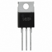
BUK9508-55A,127 NXP Semiconductors, BUK9508-55A,127 Datasheet - Page 5

BUK9508-55A,127
Manufacturer Part Number
BUK9508-55A,127
Description
MOSFET N-CH 55V 75A SOT78
Manufacturer
NXP Semiconductors
Series
TrenchMOS™r
Datasheet
1.BUK9608-55A118.pdf
(14 pages)
Specifications of BUK9508-55A,127
Fet Type
MOSFET N-Channel, Metal Oxide
Fet Feature
Logic Level Gate
Rds On (max) @ Id, Vgs
7.5 mOhm @ 25A, 10V
Drain To Source Voltage (vdss)
55V
Current - Continuous Drain (id) @ 25° C
75A
Vgs(th) (max) @ Id
2V @ 1mA
Gate Charge (qg) @ Vgs
92nC @ 5V
Input Capacitance (ciss) @ Vds
6021pF @ 25V
Power - Max
253W
Mounting Type
Through Hole
Package / Case
TO-220AB-3
Configuration
Single
Transistor Polarity
N-Channel
Resistance Drain-source Rds (on)
0.0075 Ohms
Drain-source Breakdown Voltage
55 V
Gate-source Breakdown Voltage
+/- 10 V
Continuous Drain Current
125 A
Power Dissipation
253 W
Maximum Operating Temperature
+ 175 C
Mounting Style
Through Hole
Fall Time
167 ns
Minimum Operating Temperature
- 55 C
Rise Time
175 ns
Lead Free Status / RoHS Status
Lead free / RoHS Compliant
Other names
934055644127
BUK9508-55A
BUK9508-55A
BUK9508-55A
BUK9508-55A
Philips Semiconductors
8. Characteristics
Table 5:
T
9397 750 09573
Product data
Symbol
Static characteristics
V
V
I
I
R
Dynamic characteristics
Q
Q
Q
C
C
C
t
t
t
t
L
L
DSS
GSS
d(on)
r
d(off)
f
j
d
s
(BR)DSS
GS(th)
DSon
iss
oss
rss
g(tot)
gs
gd
= 25 C unless otherwise specified.
Characteristics
Parameter
drain-source breakdown
voltage
gate-source threshold voltage I
drain-source leakage current
gate-source leakage current
drain-source on-state
resistance
total gate charge
gate-to-source charge
gate-to-drain (Miller) charge
input capacitance
output capacitance
reverse transfer capacitance
turn-on delay time
rise time
turn-off delay time
fall time
internal drain inductance
internal source inductance
Conditions
I
Figure 9
V
V
V
Figure 7
V
V
V
I
V
f = 1 MHz;
V
V
from drain lead 6 mm from
package to centre of die
from contact screw on
mounting base to centre of
die SOT78
from upper edge of drain
mounting base to centre of
die SOT404
from source lead to source
bond pad
D
D
D
DS
GS
GS
GS
GS
GS
GS
DD
GS
T
T
T
T
T
T
T
T
T
= 0.25 mA; V
= 1 mA; V
= 25 A;
j
j
j
j
j
j
j
j
j
= 55 V; V
= 25 C
= 55 C
= 25 C
= 175 C
= 55 C
= 25 C
= 175 C
= 10 V; V
= 5 V; I
= 25 C
= 175 C
= 4.5 V; I
= 10 V; I
= 5 V; V
= 0 V; V
= 30 V; R
= 5 V; R
Rev. 03 — 6 May 2002
and
Figure 14
Figure 12
D
DS
DD
DS
G
D
8
= 25 A;
D
GS
L
= 10
= 25 A
DS
= V
= 25 A
GS
= 44 V;
= 25 V;
= 1.2 ;
= 0 V
= 0 V
= 0 V
GS
;
Min
55
50
1
0.5
-
-
-
-
-
-
-
-
-
-
-
-
-
-
-
-
-
-
-
-
-
-
BUK95/9608-55A
TrenchMOS™ logic level FET
© Koninklijke Philips Electronics N.V. 2002. All rights reserved.
Typ
-
-
1.5
-
-
0.05
-
2
6.8
-
-
6.4
92
11
43
4551
760
500
40
175
280
167
4.5
3.5
2.5
7.5
Max
-
-
2
-
2.3
10
500
100
8
16
8.5
7.5
-
-
-
6021
900
687
-
-
-
-
-
-
-
-
Unit
V
V
V
V
V
nA
m
m
m
m
nC
nC
nC
pF
pF
pF
ns
ns
ns
ns
nH
nH
nH
nH
5 of 14
A
A


