IRFI744GPBF Vishay, IRFI744GPBF Datasheet

MOSFET N-CH 450V 4.9A TO220FP

IRFI744GPBF

Manufacturer Part Number
IRFI744GPBF
Description
MOSFET N-CH 450V 4.9A TO220FP
Manufacturer
Vishay
Datasheets

Specifications of IRFI744GPBF

Fet Type
MOSFET N-Channel, Metal Oxide
Fet Feature
Standard
Rds On (max) @ Id, Vgs
630 mOhm @ 2.9A, 10V
Drain To Source Voltage (vdss)
450V
Current - Continuous Drain (id) @ 25° C
4.9A
Vgs(th) (max) @ Id
4V @ 250µA
Gate Charge (qg) @ Vgs
80nC @ 10V
Input Capacitance (ciss) @ Vds
1400pF @ 25V
Power - Max
40W
Mounting Type
Through Hole
Package / Case
TO-220-3 Full Pack (Straight Leads, Isolated), ITO-220AB
Transistor Polarity
N Channel
Continuous Drain Current Id
4.9A
Drain Source Voltage Vds
450V
On Resistance Rds(on)
630mohm
Rds(on) Test Voltage Vgs
10V
Power Dissipation Pd
40W
Lead Free Status / RoHS Status
Lead free / RoHS Compliant
Other names
*IRFI744GPBF
Notes
a. Repetitive rating; pulse width limited by maximum junction temperature (see fig. 11).
b. V
c. I
d. 1.6 mm from case.
* Pb containing terminations are not RoHS compliant, exemptions may apply
Document Number: 91157
S09-0012-Rev. A, 19-Jan-09
PRODUCT SUMMARY
V
R
Q
Q
Q
Configuration
ORDERING INFORMATION
Package
Lead (Pb)-free
SnPb
ABSOLUTE MAXIMUM RATINGS T
PARAMETER
Drain-Source Voltage
Gate-Source Voltage
Continuous Drain Current
Pulsed Drain Current
Linear Derating Factor
Single Pulse Avalanche Energy
Repetitive Avalanche Current
Repetitive Avalanche Energy
Maximum Power Dissipation
Peak Diode Recovery dV/dt
Operating Junction and Storage Temperature Range
Soldering Recommendations (Peak Temperature)
Mounting Torque
DS
DS(on)
g
gs
gd
SD
TO-220 FULLPAK
DD
(Max.) (nC)
(nC)
(nC)
(V)
≤ 8.8 A, dI/dt ≤ 200 A/µs, V
= 50 V, starting T
(Ω)
a
J
G
= 25 °C, L = 9.6 mH, R
D
c
a
a
S
b
DD
V
GS
≤ V
= 10 V
DS
G
, T
N-Channel MOSFET
Single
J
450
≤ 150 °C.
80
12
41
G
= 25 Ω, I
D
S
C
Power MOSFET
= 25 °C, unless otherwise noted
V
0.63
GS
AS
6-32 or M3 screw
at 10 V
= 4.9 A (see fig. 12).
T
for 10 s
C
= 25 °C
T
T
C
C
TO-220 FULLPAK
IRFI744GPbF
SiHFI744G-E3
IRFI744G
SiHFI744G
= 100 °C
= 25 °C
FEATURES
• Isolated Package
• High Voltage Isolation = 2.5 kV
• Sink to Lead Creepage Dist. = 4.8 mm
• Dynamic dV/dt Rating
• Low Thermal Resistance
• Lead (Pb)-free Available
DESCRIPTION
Third generation Power MOSFETs from Vishay provide the
designer with the best combination of fast switching,
ruggedized
cost-effectiveness.
The TO-220 FULLPAK eliminates the need for additional
insulating hardware in commercial-industrial applications.
The molding compound used provides a high isolation
capability and a low thermal resistance between the tab and
external heatsink. This isolation is equivalent to using a 100
micron mica barrier with standard TO-220 product. The
FULLPAK is mounted to a heatsink using a single clip or by
a single screw fixing.
f = 60 Hz)
SYMBOL
T
dV/dt
J
V
V
E
E
I
I
P
, T
device
I
DM
AR
DS
GS
AS
AR
D
D
stg
IRFI744G, SiHFI744G
design,
- 55 to + 150
LIMIT
300
± 20
0.32
450
130
4.9
3.1
4.9
4.0
3.5
1.1
20
40
10
low
RMS
d
Vishay Siliconix
(t = 60 s;
on-resistance
www.vishay.com
lbf · in
UNIT
W/°C
N · m
V/ns
RoHS*
COMPLIANT
mJ
mJ
°C
W
V
A
A
Available
and
1

Related parts for IRFI744GPBF

IRFI744GPBF Summary of contents

Page 1

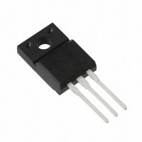
... S external heatsink. This isolation is equivalent to using a 100 micron mica barrier with standard TO-220 product. The N-Channel MOSFET FULLPAK is mounted to a heatsink using a single clip single screw fixing. TO-220 FULLPAK IRFI744GPbF SiHFI744G-E3 IRFI744G SiHFI744G = 25 °C, unless otherwise noted °C ...

Page 2

... IRFI744G, SiHFI744G Vishay Siliconix THERMAL RESISTANCE RATINGS PARAMETER Maximum Junction-to-Ambient Maximum Junction-to-Case (Drain) SPECIFICATIONS °C, unless otherwise noted J PARAMETER Static Drain-Source Breakdown Voltage V Temperature Coefficient DS Gate-Source Threshold Voltage Gate-Source Leakage Zero Gate Voltage Drain Current Drain-Source On-State Resistance Forward Transconductance Dynamic ...

Page 3

... TYPICAL CHARACTERISTICS 25 °C, unless otherwise noted Fig Typical Output Characteristics, T Fig Typical Output Characteristics, T Document Number: 91157 S09-0012-Rev. A, 19-Jan- °C Fig Typical Transfer Characteristics C = 150 °C Fig Normalized On-Resistance vs. Temperature C IRFI744G, SiHFI744G Vishay Siliconix www.vishay.com 3 ...

Page 4

... IRFI744G, SiHFI744G Vishay Siliconix Fig Typical Capacitance vs. Drain-to-Source Voltage Fig Typical Gate Charge vs. Gate-to-Source Voltage www.vishay.com 4 Fig Typical Source-Drain Diode Forward Voltage Fig Maximum Safe Operating Area Document Number: 91157 S09-0012-Rev. A, 19-Jan-09 ...

Page 5

... Fig. 12a - Unclamped Inductive Test Circuit Document Number: 91157 S09-0012-Rev. A, 19-Jan-09 IRFI744G, SiHFI744G Pulse width ≤ 1 µs Duty factor ≤ 0.1 % Fig. 10a - Switching Time Test Circuit d(on) Fig. 10b - Switching Time Waveforms + Fig. 12b - Unclamped Inductive Waveforms Vishay Siliconix D.U. d(off www.vishay.com 5 ...

Page 6

... IRFI744G, SiHFI744G Vishay Siliconix Fig. 12c - Maximum Avalanche Energy vs. Drain Current Charge Fig. 13a - Basic Gate Charge Waveform www.vishay.com 6 Current regulator Same type as D.U.T. 50 kΩ 0.2 µF 0.3 µ D.U. Current sampling resistors Fig. 13b - Gate Charge Test Circuit Document Number: 91157 ...

Page 7

... V GS Vishay Siliconix maintains worldwide manufacturing capability. Products may be manufactured at one of several qualified locations. Reliability data for Silicon Technology and Package Reliability represent a composite of all qualified locations. For related documents such as package/tape drawings, part marking, and reliability data, see www.vishay.com/ppg?91157. Document Number: 91157 S09-0012-Rev ...

Page 8

... Vishay disclaims any and all liability arising out of the use or application of any product described herein or of any information provided herein to the maximum extent permitted by law. The product specifications do not expand or otherwise modify Vishay’ ...

Related keywords