SPP11N60C3 Infineon Technologies, SPP11N60C3 Datasheet - Page 3
SPP11N60C3
Manufacturer Part Number
SPP11N60C3
Description
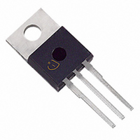
MOSFET N-CH 650V 11A TO-220AB
Manufacturer
Infineon Technologies
Series
CoolMOS™r
Datasheet
1.SPI11N60C3.pdf
(16 pages)
Specifications of SPP11N60C3
Package / Case
TO-220AB
Fet Type
MOSFET N-Channel, Metal Oxide
Fet Feature
Standard
Rds On (max) @ Id, Vgs
380 mOhm @ 7A, 10V
Drain To Source Voltage (vdss)
650V
Current - Continuous Drain (id) @ 25° C
11A
Vgs(th) (max) @ Id
3.9V @ 500µA
Gate Charge (qg) @ Vgs
60nC @ 10V
Input Capacitance (ciss) @ Vds
1200pF @ 25V
Power - Max
125W
Mounting Type
Through Hole
Minimum Operating Temperature
- 55 C
Configuration
Single
Transistor Polarity
N-Channel
Resistance Drain-source Rds (on)
0.38 Ohm @ 10 V
Drain-source Breakdown Voltage
600 V
Gate-source Breakdown Voltage
+/- 20 V
Continuous Drain Current
11 A
Power Dissipation
125000 mW
Maximum Operating Temperature
+ 150 C
Mounting Style
Through Hole
Lead Free Status / RoHS Status
Lead free / RoHS Compliant
Lead Free Status / RoHS Status
Lead free / RoHS Compliant, Lead free / RoHS Compliant
Other names
SP000013526
SPP11N60C3IN
SPP11N60C3X
SPP11N60C3XIN
SPP11N60C3XIN
SPP11N60C3XK
SPP11N60C3IN
SPP11N60C3X
SPP11N60C3XIN
SPP11N60C3XIN
SPP11N60C3XK
Available stocks
Company
Part Number
Manufacturer
Quantity
Price
Company:

Part Number:
SPP11N60C3
Manufacturer:
INFINEON
Quantity:
4 500
Company:
Part Number:
SPP11N60C3
Manufacturer:
INFINEON
Quantity:
50
Company:
Part Number:
SPP11N60C3
Manufacturer:
Infineon Technologies
Quantity:
1 818
Company:
Part Number:
SPP11N60C3XKSA1
Manufacturer:
INFINEON
Quantity:
3 000
Part Number:
SPP11N60C3XKSA1
Manufacturer:
INFINEON/英飞凌
Quantity:
20 000


Rev.
Electrical Characteristics
Parameter
Transconductance
Input capacitance
Output capacitance
Reverse transfer capacitance
Effective output capacitance,
energy related
Effective output capacitance,
time related
Turn-on delay time
Rise time
Turn-off delay time
Fall time
Gate Charge Characteristics
Gate to source charge
Gate to drain charge
Gate charge total
Gate plateau voltage
1 Limited only by maximum temperature
2 Repetitve avalanche causes additional power losses that can be calculated as P
3 Device on 40mm*40mm*1.5mm epoxy PCB FR4 with 6cm² (one layer, 70 µm thick) copper area for drain
connection. PCB is vertical without blown air.
4 Soldering temperature for TO-263: 220°C, reflow
5 C
6 C
7 ISD<=ID, di/dt<=400A/us, VDClink=400V, Vpeak<VBR, DSS, Tj<Tj,max.
Identical low-side and high-side switch.
o(er)
o(tr)
is a fixed capacitance that gives the same charging time as C
is a fixed capacitance that gives the same stored energy as C
3 .2
5)
6)
SPI11N60C3, SPA11N60C3, SPA11N60C3 E8185
g
C
C
C
C
C
t
t
t
t
Q
Q
Q
V
Symbol
d(on)
r
d(off)
f
fs
(plateau)
iss
oss
rss
o(er)
o(tr)
gs
gd
g
V
I
V
f=1MHz
V
V
V
I
R
V
V
V
V
D
D
DS
GS
GS
DS
DD
G
DD
DD
GS
DD
=7A
=11A,
=6.8Ω
≥2*I
=0V to 480V
=0V, V
=0V,
=380V, V
=480V, I
=480V, I
=0 to 10V
=480V, I
Page 3
Conditions
D
*R
DS
DS(on)max
D
D
D
GS
=25V,
=11A
=11A,
=11A
=0/10V,
oss
oss
while V
while V
,
min.
DS
DS
-
-
-
-
-
-
-
-
-
-
-
-
-
-
AV
is rising from 0 to 80% V
is rising from 0 to 80% V
=E
Values
AR
1200
typ.
390
8.3
5.5
5.5
30
45
85
10
44
22
45
*f.
5
5
SPP11N60C3
2009-11-27
max.
70
60
9
-
-
-
-
-
-
-
-
-
-
-
Unit
S
pF
ns
nC
V
DSS
DSS
.
.
Related parts for SPP11N60C3
Image
Part Number
Description
Manufacturer
Datasheet
Request
R


Part Number:
Description:
General Purpose Wirewound Resistors
Manufacturer:
Welwyn Components
Datasheet:

Part Number:
Description:
Manufacturer:
Infineon Technologies AG
Datasheet:
Part Number:
Description:
Manufacturer:
Infineon Technologies AG
Datasheet:
Part Number:
Description:
Manufacturer:
Infineon Technologies AG
Datasheet:
Part Number:
Description:
Manufacturer:
Infineon Technologies AG
Datasheet:
Part Number:
Description:
Manufacturer:
Infineon Technologies AG
Datasheet:
Part Number:
Description:
Manufacturer:
Infineon Technologies AG
Datasheet:
Part Number:
Description:
Manufacturer:
Infineon Technologies AG
Datasheet:
Part Number:
Description:
16-bit microcontroller with 2x2 KByte RAM
Manufacturer:
Infineon Technologies AG
Datasheet:
Part Number:
Description:
NPN silicon RF transistor
Manufacturer:
Infineon Technologies AG
Datasheet:
Part Number:
Description:
NPN silicon RF transistor
Manufacturer:
Infineon Technologies AG
Datasheet:
Part Number:
Description:
NPN silicon RF transistor
Manufacturer:
Infineon Technologies AG
Datasheet:
Part Number:
Description:
NPN silicon RF transistor
Manufacturer:
Infineon Technologies AG
Datasheet: