NTD4963N-1G ON Semiconductor, NTD4963N-1G Datasheet

MOSFET N-CH 30V 8.1A IPAK

NTD4963N-1G

Manufacturer Part Number
NTD4963N-1G
Description
MOSFET N-CH 30V 8.1A IPAK
Manufacturer
ON Semiconductor
Datasheet

Specifications of NTD4963N-1G

Package / Case
IPak, TO-251, DPak (3 straight short leads + tab)
Mounting Type
Through Hole
Power - Max
1.1W
Fet Type
MOSFET N-Channel, Metal Oxide
Gate Charge (qg) @ Vgs
16.2nC @ 10V
Vgs(th) (max) @ Id
2.5V @ 250µA
Current - Continuous Drain (id) @ 25° C
8.1A
Drain To Source Voltage (vdss)
30V
Fet Feature
Logic Level Gate
Rds On (max) @ Id, Vgs
9.6 mOhm @ 30A, 10V
Configuration
Single
Transistor Polarity
N-Channel
Resistance Drain-source Rds (on)
13.6 mOhms
Forward Transconductance Gfs (max / Min)
40 S
Drain-source Breakdown Voltage
30 V
Continuous Drain Current
44 A
Power Dissipation
35.7 W
Maximum Operating Temperature
+ 175 C
Mounting Style
SMD/SMT
Gate Charge Qg
8.1 nC
Minimum Operating Temperature
- 55 C
Lead Free Status / RoHS Status
Lead free / RoHS Compliant

Available stocks

Company
Part Number
Manufacturer
Quantity
Price
Part Number:
NTD4963N-1G
Manufacturer:
ON Semiconductor
Quantity:
50
Part Number:
NTD4963N-1G
Manufacturer:
ON
Quantity:
12 500
NTD4963N
Power MOSFET
30 V, 44 A, Single N−Channel, DPAK/IPAK
Features
Applications
Stresses exceeding Maximum Ratings may damage the device. Maximum
Ratings are stress ratings only. Functional operation above the Recommended
Operating Conditions is not implied. Extended exposure to stresses above the
Recommended Operating Conditions may affect device reliability.
1. Surface−mounted on FR4 board using 1 sq−in pad, 1 oz Cu.
2. Surface−mounted on FR4 board using the minimum recommended pad size.
© Semiconductor Components Industries, LLC, 2009
December, 2009 − Rev. 0
MAXIMUM RATINGS
Drain−to−Source Voltage
Gate−to−Source Voltage
Continuous Drain
Current R
(Note 1)
Power Dissipation
R
Continuous Drain
Current R
(Note 2)
Power Dissipation
R
Continuous Drain
Current R
(Note 1)
Power Dissipation
R
Pulsed Drain
Current
Current Limited by Package
Operating Junction and Storage
Temperature
Source Current (Body Diode)
Drain to Source dV/dt
Single Pulse Drain−to−Source Avalanche
Energy (T
I
Lead Temperature for Soldering Purposes
(1/8” from case for 10 s)
L
Compliant
Low R
Low Capacitance to Minimize Driver Losses
Optimized Gate Charge to Minimize Switching Losses
Three Package Variations for Design Flexibility
These Devices are Pb−Free, Halogen Free/BFR Free and are RoHS
CPU Power Delivery
DC−DC Converters
Recommended for High Side (Control)
qJA
qJA
qJC
= 26 A
(Note 1)
(Note 2)
(Note 1)
DS(on)
pk
qJA
qJA
qJC
J
, L = 0.1 mH, R
= 25°C, V
to Minimize Conduction Losses
Parameter
DD
t
Steady
p
State
=10ms
= 50 V, V
(T
G
J
= 25 W)
= 25°C unless otherwise stated)
GS
T
T
T
T
T
T
T
T
T
T
T
A
A
A
A
A
A
C
C
C
A
A
= 10 V,
= 25°C
= 85°C
= 25°C
= 25°C
= 85°C
= 25°C
= 25°C
= 85°C
= 25°C
= 25°C
= 25°C
I
Symbol
DmaxPkg
V
T
dV/dt
EAS
V
I
P
P
P
T
STG
T
DSS
ID
DM
I
I
I
GS
D
D
S
J
D
D
D
L
,
−55 to
Value
+175
10.0
1.64
35.7
33.8
±20
132
260
7.2
8.1
5.8
1.1
6.0
30
44
32
35
30
1
Unit
V/ns
mJ
°C
°C
W
W
W
V
V
A
A
A
A
A
A
Gate
See detailed ordering and shipping information in the package
dimensions section on page 3 of this data sheet.
CASE 369AA
1
1 2
(Bent Lead)
V
STYLE 2
Drain
Drain 3
(BR)DSS
30 V
DPAK
4
2
3
Source
ORDERING INFORMATION
G
Y
WW
4963N = Device Code
G
MARKING DIAGRAMS
& PIN ASSIGNMENTS
4
N−CHANNEL MOSFET
http://onsemi.com
Gate
(Straight Lead)
9.6 mW @ 10 V
16 mW @ 4.5 V
R
CASE 369AC
1
= Year
= Work Week
= Pb−Free Package
DS(ON)
Drain
Drain
3 IPAK
1
4
D
2
2 3
Publication Order Number:
3
4
MAX
Source
S
Gate
(Straight Lead
CASE 369D
1
1
NTD4963N/D
Drain
DPAK)
Drain
2
I
IPAK
D
4
44 A
3
2
MAX
3
Source
4

Related parts for NTD4963N-1G

NTD4963N-1G Summary of contents

Page 1

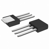
... CASE 369AC CASE 369D 3 IPAK IPAK (Straight Lead) (Straight Lead DPAK) MARKING DIAGRAMS & PIN ASSIGNMENTS 4 Drain 4 Drain Gate Drain Source Source Gate Drain Source Y = Year WW = Work Week 4963N = Device Code G = Pb−Free Package ORDERING INFORMATION Publication Order Number: NTD4963N/D ...

Page 2

THERMAL RESISTANCE MAXIMUM RATINGS Parameter Junction−to−Case (Drain) Junction−to−TAB (Drain) Junction−to−Ambient – Steady State (Note 3) Junction−to−Ambient – Steady State (Note 4) 3. Surface−mounted on FR4 board using 1 sq−in pad Cu. 4. Surface−mounted on FR4 board using the ...

Page 3

... Assume terminal length of 110 mils. ORDERING INFORMATION Device NTD4963NT4G NTD4963N−1G NTD4963N−35G IPAK Trimmed Lead †For information on tape and reel specifications, including part orientation and tape sizes, please refer to our Tape and Reel Packaging Specifications Brochure, BRD8011/ 25°C unless otherwise specified) ...

Page 4

V thru 25° DRAIN−TO−SOURCE VOLTAGE (V) DS Figure 1. On−Region Characteristics 2E−02 1.9E−02 1.8E−02 1.7E−02 1.6E−02 1.5E−02 1.4E−02 1.3E−02 1.2E−02 1.1E−02 ...

Page 5

C V iss GS 1000 800 600 400 C oss 200 C rss DRAIN−TO−SOURCE VOLTAGE (V) DS Figure 7. Capacitance Variation 1000 ...

Page 6

... 0.13 (0.005) M *For additional information on our Pb−Free strategy and soldering details, please download the ON Semiconductor Soldering and Mounting Techniques Reference Manual, SOLDERRM/D. PACKAGE DIMENSIONS DPAK (SINGLE GAUGE) CASE 369AA−01 ISSUE A SEATING −T− PLANE SOLDERING FOOTPRINT* 6.20 3.0 0.244 0.118 2 ...

Page 7

... S 0.025 0.040 0.63 1.01 V 0.035 0.050 0.89 1.27 Z 0.155 −−− 3.93 −−− STYLE 2: PIN 1. GATE 2. DRAIN 3. SOURCE 4. DRAIN ON Semiconductor Website: www.onsemi.com Order Literature: http://www.onsemi.com/orderlit For additional information, please contact your local Sales Representative NTD4963N/D ...

Related keywords