IRF7799L2TRPBF International Rectifier, IRF7799L2TRPBF Datasheet - Page 2
IRF7799L2TRPBF
Manufacturer Part Number
IRF7799L2TRPBF
Description
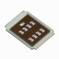
MOSFET N-CH 250V DIRECTFET L8
Manufacturer
International Rectifier
Series
HEXFET®r
Datasheet
1.IRF7799L2TRPBF.pdf
(11 pages)
Specifications of IRF7799L2TRPBF
Fet Type
MOSFET N-Channel, Metal Oxide
Fet Feature
Standard
Rds On (max) @ Id, Vgs
38 mOhm @ 21A, 10V
Drain To Source Voltage (vdss)
250V
Current - Continuous Drain (id) @ 25° C
375A
Vgs(th) (max) @ Id
5V @ 250µA
Gate Charge (qg) @ Vgs
165nC @ 10V
Input Capacitance (ciss) @ Vds
6714pF @ 25V
Power - Max
4.3W
Mounting Type
Surface Mount
Package / Case
DirectFET™ Isometric L8
Transistor Polarity
N-Channel
Drain-source Breakdown Voltage
250 V
Gate-source Breakdown Voltage
30 V
Continuous Drain Current
35 A
Power Dissipation
125 W
Gate Charge Qg
110 nC
Lead Free Status / RoHS Status
Lead free / RoHS Compliant
Available stocks
Company
Part Number
Manufacturer
Quantity
Price
Company:

Part Number:
IRF7799L2TRPBF
Manufacturer:
UCHIHASHI
Quantity:
10 000


BV
∆ΒV
R
V
∆V
I
I
gfs
Q
Q
Q
R
t
t
t
t
C
C
C
C
C
I
I
V
t
Q
Static @ T
Diode Characteristics
DSS
GSS
d(on)
r
d(off)
f
S
SM
rr
DS(on)
GS(th)
G
iss
oss
rss
oss
oss
SD
g
Q
Q
Q
Q
sw
oss
rr
2
GS(th)
DSS
gs1
gs2
gd
godr
DSS
/∆T
/∆T
J
J
J
= 25°C (unless otherwise specified)
Drain-to-Source Breakdown Voltage
Breakdown Voltage Temp. Coefficient
Static Drain-to-Source On-Resistance
Gate Threshold Voltage
Gate Threshold Voltage Coefficient
Drain-to-Source Leakage Current
Gate-to-Source Forward Leakage
Gate-to-Source Reverse Leakage
Forward Transconductance
Total Gate Charge
Pre-Vth Gate-to-Source Charge
Post-Vth Gate-to-Source Charge
Gate-to-Drain Charge
Gate Charge Overdrive
Switch Charge (Q
Output Charge
Gate Resistance
Turn-On Delay Time
Rise Time
Turn-Off Delay Time
Fall Time
Input Capacitance
Output Capacitance
Reverse Transfer Capacitance
Output Capacitance
Output Capacitance
Continuous Source Current
(Body Diode)
Pulsed Source Current
(Body Diode)
Diode Forward Voltage
Reverse Recovery Time
Reverse Recovery Charge
Parameter
Parameter
g
gs2
+ Q
gd
)
Min. Typ. Max. Units
Min. Typ. Max. Units
250
–––
–––
–––
–––
–––
–––
–––
–––
–––
–––
–––
–––
–––
–––
–––
–––
–––
–––
–––
–––
–––
–––
–––
–––
–––
–––
–––
–––
3.0
–––
54
6714
5063
1412
0.12
0.73
36.3
33.5
73.9
26.6
–––
–––
–––
–––
–––
–––
110
606
157
217
–––
–––
–––
132
4.0
-13
5.7
32
26
39
39
45
33
2118
-100
–––
–––
–––
100
–––
165
–––
–––
–––
–––
–––
–––
–––
–––
–––
–––
–––
–––
–––
–––
–––
140
198
5.0
1.3
38
20
35
1
mV/°C
V/°C
1mA
mΩ
µA
nA
nC
nC
nC
ns
pF
ns
V
V
S
Ω
A
V
V
Reference to 25°C, I
V
V
V
V
V
V
V
V
V
I
See Fig. 9
V
V
I
R
V
V
ƒ = 1.0MHz
V
V
MOSFET symbol
showing the
integral reverse
p-n junction diode.
T
T
di/dt = 100A/µs
D
D
GS
GS
DS
DS
DS
GS
GS
DS
DS
GS
DS
DD
GS
DS
GS
GS
J
J
G
= 21A
= 21A
=6.2Ω
= 25°C, I
= 25°C, I
= 0V, I
= 10V, I
= V
= 250V, V
= 250V, V
= 20V
= -20V
= 50V, I
= 125V
= 10V
= 16V, V
= 125V, V
= 0V
= 25V
= 0V, V
= 0V, V
GS
, I
D
Conditions
D
Conditions
S
F
DS
DS
D
D
= 250µA
GS
= 21A, V
= 21A, V
= 250µA
= 21A
= 21A
GS
GS
GS
= 1.0V, f=1.0MHz
= 80V, f=1.0MHz
= 0V
i
= 0V
= 0V, T
= 10V
i
D
DD
GS
www.irf.com
= 2mA
J
= 50V
= 0V
i
= 125°C
i
Related parts for IRF7799L2TRPBF
Image
Part Number
Description
Manufacturer
Datasheet
Request
R

Part Number:
Description:
SCHOTTKY RECTIFIER
Manufacturer:
International Rectifier Corp.
Datasheet:
Part Number:
Description:
SCHOTTKY RECTIFIER
Manufacturer:
International Rectifier Corp.
Datasheet:
Part Number:
Description:
SCHOTTKY RECTIFIER
Manufacturer:
International Rectifier Corp.
Datasheet:
Part Number:
Description:
SCHOTTKY RECTIFIER
Manufacturer:
International Rectifier Corp.
Datasheet:
Part Number:
Description:
SCHOTTKY RECTIFIER
Manufacturer:
International Rectifier Corp.
Datasheet:
Part Number:
Description:
SCHOTTKY RECTIFIER
Manufacturer:
International Rectifier Corp.
Datasheet:
Part Number:
Description:
SCHOTTKY RECTIFIER
Manufacturer:
International Rectifier Corp.
Datasheet:
Part Number:
Description:
SCHOTTKY RECTIFIER
Manufacturer:
International Rectifier Corp.
Datasheet:
Part Number:
Description:
SCHOTTKY RECTIFIER
Manufacturer:
International Rectifier Corp.
Datasheet:
Part Number:
Description:
SCHOTTKY RECTIFIER
Manufacturer:
International Rectifier Corp.
Datasheet:
Part Number:
Description:
SCHOTTKY RECTIFIER
Manufacturer:
International Rectifier Corp.
Datasheet:
Part Number:
Description:
SCHOTTKY RECTIFIER
Manufacturer:
International Rectifier Corp.
Datasheet:
Part Number:
Description:
SCHOTTKY RECTIFIER
Manufacturer:
International Rectifier Corp.
Datasheet:
Part Number:
Description:
SCHOTTKY RECTIFIER
Manufacturer:
International Rectifier Corp.
Datasheet:
Part Number:
Description:
SCHOTTKY RECTIFIER
Manufacturer:
International Rectifier Corp.
Datasheet: