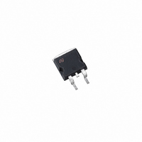
STB100NF04T4 STMicroelectronics, STB100NF04T4 Datasheet - Page 4

STB100NF04T4
Manufacturer Part Number
STB100NF04T4
Description
MOSFET N-CH 40V 120A D2PAK
Manufacturer
STMicroelectronics
Series
STripFET™r
Datasheet
1.STP100NF04.pdf
(17 pages)
Specifications of STB100NF04T4
Fet Type
MOSFET N-Channel, Metal Oxide
Fet Feature
Standard
Rds On (max) @ Id, Vgs
4.6 mOhm @ 50A, 10V
Drain To Source Voltage (vdss)
40V
Current - Continuous Drain (id) @ 25° C
120A
Vgs(th) (max) @ Id
4V @ 250µA
Gate Charge (qg) @ Vgs
150nC @ 10V
Input Capacitance (ciss) @ Vds
5100pF @ 25V
Power - Max
300W
Mounting Type
Surface Mount
Package / Case
D²Pak, TO-263 (2 leads + tab)
Configuration
Single
Transistor Polarity
N-Channel
Resistance Drain-source Rds (on)
0.0046 Ohm @ 10 V
Forward Transconductance Gfs (max / Min)
150 S
Drain-source Breakdown Voltage
40 V
Gate-source Breakdown Voltage
+/- 20 V
Continuous Drain Current
120 A
Power Dissipation
300000 mW
Maximum Operating Temperature
+ 175 C
Mounting Style
SMD/SMT
Minimum Operating Temperature
- 55 C
Lead Free Status / RoHS Status
Lead free / RoHS Compliant
Other names
497-5951-2
Available stocks
Company
Part Number
Manufacturer
Quantity
Price
Company:
Part Number:
STB100NF04T4
Manufacturer:
STMicroelectronics
Quantity:
2 250
Electrical characteristics
2
4/17
Electrical characteristics
(T
Table 3.
Table 4.
Symbol
V
CASE
Symbol
R
V
t
t
(BR)DSS
C
C
C
Q
Q
d(on)
d(off)
gfs
I
I
Q
DS(on)
GS(th)
DSS
GSS
oss
t
t
rss
iss
gs
gd
r
f
g
=25°C unless otherwise specified)
Forward Transconductance
Input Capacitance
Output Capacitance
Reverse Transfer Capacitance
Total Gate Charge
Gate-Source Charge
Gate-Drain Charge
Turn-on Delay Time
Rise time
Turn-off delay Time
Fall Time
On/off
Dynamic
Drain-source Breakdown
Voltage
Zero Gate Voltage Drain
Current (V
Gate-body Leakage
Current (V
Gate Threshold Voltage
Static Drain-source On
Resistance
Parameter
Parameter
GS
DS
=0)
=0)
I
V
V
V
V
V
D
GS
GS
DS
DS
DS
=250µA, V
=Max Rating
=Max Rating Tc=125°C
=±20V
=V
=10V, I
V
V
V
V
V
R
(see
GS
DS
DS
DD
DD
GS,
G
Test conditions
=4.7Ω , V
=15V, I
=25V, f=1MHz,V
=32V, I
=10V
=20V, I
Test conditions
Figure
I
D
D
=250µA
=50A
GS
=0
D
D
D
GS
21)
=50A
=120A
=60A
=10V
GS
=0
STB100NF04 - STP100NF04
Min.
Min
40
2
0.0043 0.0046
5100
1300
Typ.
Typ.
150
160
110
220
35
70
35
80
50
Max.
Max.
±100
150
10
1
4
Unit
Unit
µA
µA
nA
nC
nC
nC
pF
pF
pF
ns
ns
ns
ns
V
V
Ω
S


