IRF6637 International Rectifier, IRF6637 Datasheet

MOSFET N-CH 30V 14A DIRECTFET

IRF6637

Manufacturer Part Number
IRF6637
Description
MOSFET N-CH 30V 14A DIRECTFET
Manufacturer
International Rectifier
Series
HEXFET®r
Datasheet

Specifications of IRF6637

Fet Type
MOSFET N-Channel, Metal Oxide
Fet Feature
Logic Level Gate
Rds On (max) @ Id, Vgs
7.7 mOhm @ 14A, 10V
Drain To Source Voltage (vdss)
30V
Current - Continuous Drain (id) @ 25° C
14A
Vgs(th) (max) @ Id
2.35V @ 250µA
Gate Charge (qg) @ Vgs
17nC @ 4.5V
Input Capacitance (ciss) @ Vds
1330pF @ 15V
Power - Max
2.3W
Mounting Type
Surface Mount
Package / Case
DirectFET™ Isometric MP
Configuration
Single Quad Drain Dual Source
Transistor Polarity
N-Channel
Resistance Drain-source Rds (on)
7.7 m Ohms
Drain-source Breakdown Voltage
30 V
Gate-source Breakdown Voltage
+/- 20 V
Continuous Drain Current
14 A
Power Dissipation
2.3 W
Maximum Operating Temperature
+ 150 C
Mounting Style
Through Hole
Fall Time
3.8 ns
Minimum Operating Temperature
- 40 C
Rise Time
15 ns
Lead Free Status / RoHS Status
Contains lead / RoHS non-compliant

Available stocks

Company
Part Number
Manufacturer
Quantity
Price
Part Number:
IRF6637 (94-3605)-Q
Manufacturer:
IR
Quantity:
2 145
Part Number:
IRF6637TR1
Manufacturer:
IR
Quantity:
20 000
Company:
Part Number:
IRF6637TR1
Quantity:
990
Part Number:
IRF6637TR1PBF
Manufacturer:
SHARP
Quantity:
3 000
Part Number:
IRF6637TRPBF
Manufacturer:
IR
Quantity:
20 000
l
l
l
l
l
l
l
l
l
Description
The IRF6637 combines the latest HEXFET® power MOSFET silicon technology with advanced DirectFET
on-state resistance in a package that has the footprint of a SO-8 and only 0.7 mm profile. The DirectFET package is compatible with existing
layout geometries used in power applications, PCB assembly equipment and vapor phase, infra-red or convection soldering techniques,
when application note AN-1035 is followed regarding the manufacturing methods and processes. The DirectFET package allows dual sided
cooling to maximize thermal transfer in power systems, improving previous best thermal resistance by 80%.
The IRF6637 balances both low resistance and low charge along with ultra low package inductance to reduce both conduction and switching
losses. The reduced total losses make this product ideal for high efficiency DC-DC converters that power the latest generation of processors
operating at higher frequencies. The IRF6637 has been optimized for parameters that are critical in synchronous buck operating from 12 volt
bus converters including R
Applicable DirectFET Outline and Substrate Outline (see p.7,8 for details)

ƒ
Notes:
www.irf.com
Absolute Maximum Ratings
V
V
I
I
I
I
E
I
D
D
D
DM
AR
DS
GS
AS
Lead and Bromide Free 
Low Profile (<0.7 mm)
Dual Sided Cooling Compatible 
Ultra Low Package Inductance
Optimized for High Frequency Switching 
Ideal for CPU Core DC-DC Converters
Optimized for Control FET
Low Conduction and Switching Losses
Compatible with Existing Surface Mount Techniques 
Applications
Click on this section to link to the appropriate technical paper.
Click on this section to link to the DirectFET Website.
Surface mounted on 1 in. square Cu board, steady state.
@ T
@ T
@ T
SQ
A
A
C
= 25°C
= 70°C
= 25°C
25
20
15
10
5
2.0
Fig 1. Typical On-Resistance Vs. Gate Voltage
SX
V GS , Gate-to-Source Voltage (V)
T J = 25°C
4.0
DS(on)
Drain-to-Source Voltage
Gate-to-Source Voltage
Continuous Drain Current, V
Pulsed Drain Current
Single Pulse Avalanche Energy
Avalanche Current
ST
and gate charge to minimize losses in the control FET socket.
6.0
T J = 125°C
Ãg
8.0
I D = 14A
g
Parameter
GS
GS
GS
MQ
10.0
@ 10V
@ 10V
@ 10V
h
f
MX
30V max ±20V max 5.7mΩ@ 10V 8.2mΩ@ 4.5V
Q
11nC
T
Repetitive rating; pulse width limited by max. junction temperature.
Starting T
V
C
g tot
DSS
measured with thermocouple mounted to top (Drain) of part.
MT
Fig 2. Typical Total Gate Charge vs Gate-to-Source Voltage
12
10
8
6
4
2
0

J
4.0nC
0
= 25°C, L = 0.52mH, R
Q
I D = 11A
gd
V
DirectFET™ Power MOSFET ‚
GS
4
MP
MP
Q G Total Gate Charge (nC)
1.0nC
Q
gs2
8
Max.
V DS = 24V
VDS= 15V
110
±20
30
14
11
59
31
11
TM
R
packaging to achieve the lowest
12
DS(on)
G
20nC
Q
= 25Ω, I
rr
IRF6637
16
DirectFET™ ISOMETRIC
AS
9.9nC
Q
= 11A.
oss
20
R
DS(on)
Units
V
24
mJ
1.8V
V
A
A
gs(th)
1
4/17/06

Related parts for IRF6637

IRF6637 Summary of contents

Page 1

... The reduced total losses make this product ideal for high efficiency DC-DC converters that power the latest generation of processors operating at higher frequencies. The IRF6637 has been optimized for parameters that are critical in synchronous buck operating from 12 volt bus converters including R and gate charge to minimize losses in the control FET socket ...

Page 2

... IRF6637 Static @ T = 25°C (unless otherwise specified) J Parameter BV Drain-to-Source Breakdown Voltage DSS ∆ΒV /∆T Breakdown Voltage Temp. Coefficient DSS J R Static Drain-to-Source On-Resistance DS(on) V Gate Threshold Voltage GS(th) ∆V /∆T Gate Threshold Voltage Coefficient GS(th Drain-to-Source Leakage Current DSS I Gate-to-Source Forward Leakage ...

Page 3

... Notes: 1. Duty Factor D = t1/t2 2. Peak Zthja + Tc 0 ƒ J ‰ Mounted on minimum with footprint full size board with metalized back and with small clip heatsink (still air) IRF6637 Units W °C Units °C/W W/°C 100 3 ...

Page 4

... IRF6637 1000 100 10 1 ≤60µs PULSE WIDTH 2. 25°C 0.1 0 Drain-to-Source Voltage (V) Fig 4. Typical Output Characteristics 1000 15V ≤60µs PULSE WIDTH 100 150° 25° -40°C 1 0.1 1.5 2.0 2.5 3 Gate-to-Source Voltage (V) Fig 6. Typical Transfer Characteristics 10000 0V MHZ C iss = SHORTED ...

Page 5

... 1.0 1.2 125 150 Fig 13. Typical Threshold Voltage vs. Junction 160 TOP 120 BOTTOM 100 Starting Junction Temperature (°C) IRF6637 1000 OPERATION IN THIS AREA LIMITED (on) 100 100µsec 1msec 10 10msec 25° 150°C Single Pulse 0.1 0.10 1.00 10. Drain-to-Source Voltage (V) Fig11. Maximum Safe Operating Area 2 ...

Page 6

... IRF6637 0 1K Fig 15a. Gate Charge Test Circuit D.U 20V 0.01 Ω Fig 16a. Unclamped Inductive Test Circuit Pulse Width < 1µs Duty Factor < 0.1% Fig 17a. Switching Time Test Circuit 6 L VCC DUT 15V DRIVER + 90 D.U.T Vds Vgs(th) Qgs1 Qgs2 ...

Page 7

... D.U. Re-Applied + Voltage - Inductor Curent V ® HEXFET Power MOSFETs P.W. Period D = Period Waveform SD Body Diode Forward Current di/dt Waveform DS Diode Recovery dv/dt Body Diode Forward Drop Ripple ≤ for Logic Level Devices for N-Channel G = GATE D= DRAIN S = SOURCE D D IRF6637 V =10V ...

Page 8

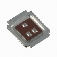
... IRF6637 DirectFET™ Outline Dimension, MP Outline (Medium Size Can, P-Designation). Please see DirectFET application note AN-1035 for all details regarding the assembly of DirectFET. This includes all recommendations for stencil and substrate designs. DirectFET™ Part Marking 8 DIMENSIONS IMPERIAL METRIC MAX CODE ...

Page 9

... DirectFET™ Tape & Reel Dimension (Showing component orientation). NOTE: Controlling dimensions in mm Std reel quantity is 4800 parts. (ordered as IRF6637). For 1000 parts on 7" reel, CODE IR WORLD HEADQUARTERS: 233 Kansas St., El Segundo, California 90245, USA Tel: (310) 252-7105 www.irf.com order IRF6637TR1 ...

Page 10

Note: For the most current drawings please refer to the IR website at: http://www.irf.com/package/ ...

Related keywords