STD1NK60T4 STMicroelectronics, STD1NK60T4 Datasheet
STD1NK60T4
Specifications of STD1NK60T4
Available stocks


Related parts for STD1NK60T4


STD1NK60T4 Summary of contents
Page 1
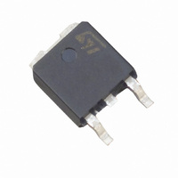
... FETs including revolutionary MDmesh™ products. APPLICATIONS LOW POWER BATTERY CHARGERS SWITH MODE LOW POWER SUPPLIES(SMPS) LOW POWER, BALLAST, CFL (COMPACT FLUORESCENT LAMPS) Table 2: Order Codes Part Number STD1NK60T4 STD1NK60-1 STQ1HNK60R STQ1HNK60R-AP STN1HNK60 February 2006 STD1NK60 - STD1NK60-1 STQ1HNK60R - STN1HNK60 Figure 1: Package ...
Page 2
STD1NK60 - STD1NK60-1 - STQ1HNK60R - STN1HNK60 Table 3: Absolute Maximum ratings Symbol V Drain-source Voltage ( Drain-gate Voltage (R DGR V Gate- source Voltage GS I Drain Current (continuous Drain Current (continuous) at ...
Page 3
ELECTRICAL CHARACTERISTICS (CONTINUED) Table 7: Dynamic Symbol Parameter g (1) Forward Transconductance fs C Input Capacitance iss Output Capacitance C oss Reverse Transfer Capacitance C rss t Turn-on Delay Time d(on) Rise Time t r Turn-off Delay Time t d(off) ...
Page 4
STD1NK60 - STD1NK60-1 - STQ1HNK60R - STN1HNK60 Figure 3: Safe Operating Area For SOT-223 . Figure 4: Safe Operating Area For DPAK/IPAK Figure 5: Safe Operating Area For TO-92 4/15 Figure 6: Thermal Impedance For SOT-223 Figure 7: Thermal Impedance ...
Page 5
Figure 9: Output Characteristics Figure 10: Transconductance Figure 11: Capacitance Variations STD1NK60 - STD1NK60-1 - STQ1HNK60R - STN1HNK60 Figure 12: Transfer Characteristics Figure 13: Gate Charge vs Gate-source Voltage Figure 14: Static Drain-source On Resistance 5/15 ...
Page 6
STD1NK60 - STD1NK60-1 - STQ1HNK60R - STN1HNK60 Figure 15: Normalized Gate Thereshold Volt- age vs Temperature Figure 16: Source-Drain Forward Characteris- tics Figure 17: Maximum Avalanche Energy vs Temperature 6/15 Figure 18: Normalized On Resistance vs Tem- perature Figure 19: ...
Page 7
Figure 21: Switching Times Test Circuit For Resistive Load Figure 22: Test Circuit For Inductive Load Switching and Diode Recovery Times STD1NK60 - STD1NK60-1 - STQ1HNK60R - STN1HNK60 Figure 23: Gate Charge Test Circuit 7/15 ...
Page 8
STD1NK60 - STD1NK60-1 - STQ1HNK60R - STN1HNK60 DIM. MIN. A 4.32 b 0.36 D 4.45 E 3.30 e 2.41 e1 1.14 L 12.70 R 2.16 S1 0.92 W 0.41 V 8/15 TO-92 MECHANICAL DATA mm. TYP MAX. MIN. 4.95 0.170 ...
Page 9
STD1NK60 - STD1NK60-1 - STQ1HNK60R - STN1HNK60 mm. DIM. MIN. TYP A1 4. 0.41 P0 12.5 12.7 P2 5.65 6.35 F1, F2 2.44 2.54 delta 17 5 8.5 ...
Page 10
STD1NK60 - STD1NK60-1 - STQ1HNK60R - STN1HNK60 DIM. MIN 0.60 B1 2.90 c 0. 3. 10/15 SOT-223 MECHANICAL DATA mm TYP. MAX. MIN. 1.80 0.70 0.80 0.024 3.00 3.10 ...
Page 11
STD1NK60 - STD1NK60-1 - STQ1HNK60R - STN1HNK60 TO-252 (DPAK) MECHANICAL DATA mm DIM. MIN. TYP. A 2.20 A1 0.90 A2 0.03 B 0.64 B2 5.20 C 0.45 C2 0.48 D 6.00 E 6.40 G 4.40 H 9.35 L2 0.8 L4 ...
Page 12
STD1NK60 - STD1NK60-1 - STQ1HNK60R - STN1HNK60 DIM. MIN. A 2.2 A1 0.9 A3 0.7 B 0. 0. 6.4 G 4 0.8 L2 12/15 ...
Page 13
STD1NK60 - STD1NK60-1 - STQ1HNK60R - STN1HNK60 DPAK FOOTPRINT All dimensions are in millimeters TAPE AND REEL SHIPMENT TAPE MECHANICAL DATA mm inch DIM. MIN. MAX. MIN. MAX. A0 6.8 7 0.267 0.275 B0 10.4 10.6 0.409 0.417 B1 12.1 ...
Page 14
STD1NK60 - STD1NK60-1 - STQ1HNK60R - STN1HNK60 Table 9: Revision History Date Revision 22-Nov-2004 2 14-Feb-2006 3 14/15 Description of Changes Added SOT-223 Package and new stylesheet Modified marking on Table 2 ...
Page 15
... No license is granted by implication or otherwise under any patent or patent rights of STMicroelectronics. Specifications mentioned in this publication are subject to change without notice. This publication supersedes and replaces all information previously supplied. STMicroelectronics products are not authorized for use as critical components in life support devices or systems without express written approval of STMicroelectronics ...