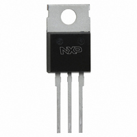
BUK7510-100B,127 NXP Semiconductors, BUK7510-100B,127 Datasheet - Page 5

BUK7510-100B,127
Manufacturer Part Number
BUK7510-100B,127
Description
MOSFET N-CH 100V 75A TO220AB
Manufacturer
NXP Semiconductors
Series
TrenchMOS™r
Datasheet
1.BUK7510-100B127.pdf
(16 pages)
Specifications of BUK7510-100B,127
Package / Case
TO-220AB-3
Mounting Type
Through Hole
Power - Max
300W
Fet Type
MOSFET N-Channel, Metal Oxide
Gate Charge (qg) @ Vgs
80nC @ 10V
Vgs(th) (max) @ Id
4V @ 1mA
Current - Continuous Drain (id) @ 25° C
75A
Drain To Source Voltage (vdss)
100V
Fet Feature
Standard
Rds On (max) @ Id, Vgs
10 mOhm @ 25A, 10V
Minimum Operating Temperature
- 55 C
Configuration
Single
Transistor Polarity
N-Channel
Resistance Drain-source Rds (on)
0.01 Ohm @ 10 V
Drain-source Breakdown Voltage
100 V
Gate-source Breakdown Voltage
20 V
Continuous Drain Current
110 A
Power Dissipation
300000 mW
Maximum Operating Temperature
+ 175 C
Mounting Style
SMD/SMT
Lead Free Status / RoHS Status
Lead free / RoHS Compliant
Lead Free Status / RoHS Status
Lead free / RoHS Compliant, Lead free / RoHS Compliant
Other names
934057110127::BUK7510-100B::BUK7510-100B
KGD program
KGD for high-current & high-temperature applications
NXP’s Known Good Die (KDG) technology overcomes the
inspection and testing issues traditionally associated with the
bare-die, wafer-based products typically needed for high-
current and high-temperature applications.
NXP’s specialized process first singulates the wafer into
individual dice, then subjects each one to a rigorous test and
inspection before final packaging into tape & reel format,
ensuring the highest possible product quality.
KGD technology enables custom mounting and bonding for
maximum contact with the die, significantly reducing R
and offering greatly reduced thermal resistance due to the
optimized thermal path to the heatsink. Free of the limitations
of standard packaging KGD also offers both high-current
(>200 A typ) and high-temperature (>175 °C typ) operation.
KGD Features and Benefits
KGD test nest
*
Testing
Inspection
Die & packaging
Courtesy of Ismeca SA
Possibility of die scratching after test
*
Test after singulation
Visually inspected
High-current test
Ruggedness test
Percentage test
Test
}
}
}
}
}
}
}
Customized probe cards with a single clamping mechanism ensure maximum die contact with minimal mechanical
handling
Singulated die electrically tested twice to guarantee datasheet specifications
Dynamic PAT/SYA to guarantee the removal of abnormal devices
High-current avalanche ruggedness testing
Automatic optical inspection pre- and post-singulation to reduce process and handling imperfections
Die sizes ranging from 2.4 to 58 mm
Dry-packed tape-and-reel delivery format
Visual inspection & test system
DS(ON)
This state-of the art technology offers a cost-effective solution
in parallel configuration, for example, in hybrid modules where
space is at a premium.
NXP’s KGD program is well established and offers large-
scale production capacity. In addition to a wide choice of
existing products NXP also supports custom KGD designs to
meet specific requirements. Delivering the highest levels of
quality and reliability, all the products in the KGD portfolio are
qualified to the AEC-Q101 standard.
Target applications for KGD products
}
}
}
}
}
2
Advanced power-steering modules
Advanced braking systems
Coolant pumps
Hybrid vehicles (with integrated and non-integrated stop/
start solutions)
Engine and transmission controllers
Yes ( manual )
Sawn Wafer
100 ( preset )
Higher
*
No
No
No
Delivery on tape and reel
Power MOSFETs for Automotive Applications
Yes ( auto optical )
200 ( T1, T2 )
NXP KGD
Lower
Yes
Yes
Yes
5


