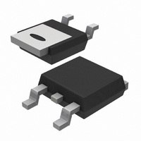
PSMN025-100D,118 NXP Semiconductors, PSMN025-100D,118 Datasheet

PSMN025-100D,118
Specifications of PSMN025-100D,118
PSMN025-100D /T3
PSMN025-100D /T3
Related parts for PSMN025-100D,118
PSMN025-100D,118 Summary of contents
Page 1
... PSMN025-100D N-channel TrenchMOS SiliconMAX standard level FET Rev. 03 — 20 November 2008 1. Product profile 1.1 General description SiliconMAX standard level N-channel enhancement mode Field-Effect Transistor (FET plastic package using TrenchMOS technology. This product is designed and qualified for use in computing, communications, consumer and industrial applications only. ...
Page 2
... kΩ 100 °C; see Figure °C; see Figure GS mb pulsed °C; see Figure °C; see Figure °C mb pulsed °C mb Rev. 03 — 20 November 2008 PSMN025-100D Graphic symbol mbb076 2 3 Version SOT428 Min Max - 100 - 100 - see Figure 188 - 150 -55 175 -55 175 ...
Page 3
... Safe operating area; continuous and peak drain currents as a function of drain-source voltage Maximum Avalanche Current, I 100 lma015 10 1 0.001 125 150 175 Fig 4. Maximum permissible non-repetitive avalanche current as a function of avalanche time Rev. 03 — 20 November 2008 PSMN025-100D Min Max ≤ 260 sup = 50 Ω 100 D.C. ...
Page 4
... Transient thermal impedance, Zth j-mb (K/ 0.5 0.2 0.1 0.1 0.05 0. single pulse 1E-06 1E-05 1E-04 1E-03 1E-02 Pulse width, tp (s) Rev. 03 — 20 November 2008 PSMN025-100D Min Typ Max - lma018 1E-01 1E+00 © NXP B.V. 2008. All rights reserved. Unit K/W ...
Page 5
... 5.6 Ω °C G(ext) j measured from tab to centre of die °C j measured from source lead to source bond pad ° °C; see Figure /dt = -100 A/µ ° Rev. 03 — 20 November 2008 PSMN025-100D Min Typ Max Unit 100 - - 0.05 10 µ 500 µA - 0.02 100 nA - 0.02 ...
Page 6
... V 0.12 0.1 0.08 0.06 0.04 0. 100 120 140 160 180 Fig 11. Drain-source on-state resistance as a function of drain current; typical values Rev. 03 — 20 November 2008 PSMN025-100D Drain current, ID (A) Forward transconductance as a function of Drain current, ID (A) minimum typical maximum 0 0 ...
Page 7
... 0.1 0.2 0.3 0.4 0.5 0.6 0.7 0.8 0.9 1 Fig 15. Source current as a function of source-drain voltage; typical values Rev. 03 — 20 November 2008 PSMN025-100D lma026 Ciss Coss Crss 1 10 Drain-Source Voltage, VDS (V) lma028 175 1.1 1.2 1.3 1.4 1.5 Source-Drain Voltage, VSDS (V) © ...
Page 8
... min min 0.56 6.22 6.73 4.0 4.45 2.285 0.20 5.98 6.47 REFERENCES JEDEC JEITA TO-252 SC-63 Rev. 03 — 20 November 2008 PSMN025-100D min 10.4 2.95 0.9 0.5 4.57 9.6 2.55 0.5 EUROPEAN ISSUE DATE PROJECTION 06-02-14 06-03-16 © NXP B.V. 2008. All rights reserved. ...
Page 9
... PSMN025-100D_1 19990201 PSMN025-100D_3 Product data sheet N-channel TrenchMOS SiliconMAX standard level FET Data sheet status Change notice Product data sheet - Product data sheet - Objective data sheet - Rev. 03 — 20 November 2008 PSMN025-100D Supersedes PSMN025-100D_2 PSMN025-100D_1 - © NXP B.V. 2008. All rights reserved ...
Page 10
... Trademarks Notice: All referenced brands, product names, service names and trademarks are the property of their respective owners. TrenchMOS — trademark of NXP B.V. http://www.nxp.com salesaddresses@nxp.com Rev. 03 — 20 November 2008 PSMN025-100D © NXP B.V. 2008. All rights reserved ...
Page 11
... Please be aware that important notices concerning this document and the product(s) described herein, have been included in section ‘Legal information’. © NXP B.V. 2008. For more information, please visit: http://www.nxp.com For sales office addresses, please send an email to: salesaddresses@nxp.com Date of release: Rev. 03 — 20 November 2008 All rights reserved. Document identifier: PSMN025-100D_3 ...


