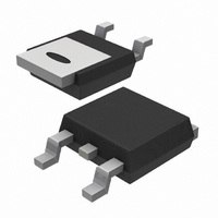
BUK9219-55A,118 NXP Semiconductors, BUK9219-55A,118 Datasheet - Page 4

BUK9219-55A,118
Manufacturer Part Number
BUK9219-55A,118
Description
MOSFET N-CH 55V 55A DPAK
Manufacturer
NXP Semiconductors
Series
TrenchMOS™r
Datasheet
1.BUK9219-55A118.pdf
(14 pages)
Specifications of BUK9219-55A,118
Package / Case
DPak, TO-252 (2 leads+tab), SC-63
Fet Type
MOSFET N-Channel, Metal Oxide
Fet Feature
Logic Level Gate
Rds On (max) @ Id, Vgs
17.6 mOhm @ 25A, 10V
Drain To Source Voltage (vdss)
55V
Current - Continuous Drain (id) @ 25° C
55A
Vgs(th) (max) @ Id
2V @ 1mA
Input Capacitance (ciss) @ Vds
2920pF @ 25V
Power - Max
114W
Mounting Type
Surface Mount
Minimum Operating Temperature
- 55 C
Configuration
Single Dual Drain
Transistor Polarity
N-Channel
Resistance Drain-source Rds (on)
0.0176 Ohm @ 10 V
Drain-source Breakdown Voltage
55 V
Gate-source Breakdown Voltage
+/- 10 V
Continuous Drain Current
55 A
Power Dissipation
114000 mW
Maximum Operating Temperature
+ 175 C
Mounting Style
SMD/SMT
Lead Free Status / RoHS Status
Lead free / RoHS Compliant
Gate Charge (qg) @ Vgs
-
Lead Free Status / Rohs Status
Lead free / RoHS Compliant
Other names
934056240118
BUK9219-55A /T3
BUK9219-55A /T3
BUK9219-55A /T3
BUK9219-55A /T3
NXP Semiconductors
BUK9219-55A
Product data sheet
Fig 1.
Fig 3.
I
(%)
der
120
80
40
0
function of mounting base temperature
Normalized continuous drain current as a
Safe operating area; continuous and peak drain currents as a function of drain-source voltage
0
50
(A)
I
D
10
10
10
1
3
2
1
P
100
R
DSon
t
p
T
= V
DS
δ =
150
/ I
T
t
t
p
D
All information provided in this document is subject to legal disclaimers.
T
mb
03aa24
(°C)
200
Rev. 02 — 7 June 2010
D.C.
10
Fig 2.
P
(%)
der
120
80
40
0
function of mounting base temperature
Normalized total power dissipation as a
0
V
N-channel TrenchMOS logic level FET
DS
50
(V)
t
100 μs
1 ms
10 ms
100 ms
p
BUK9219-55A
100
= 10μs
03nb64
10
2
150
© NXP B.V. 2010. All rights reserved.
T
mb
03aa16
(°C)
200
4 of 14


