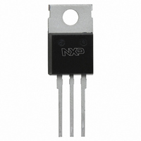
BUK95150-55A,127 NXP Semiconductors, BUK95150-55A,127 Datasheet - Page 2

BUK95150-55A,127
Manufacturer Part Number
BUK95150-55A,127
Description
MOSFET N-CH 55V 13A TO220AB
Manufacturer
NXP Semiconductors
Series
TrenchMOS™r
Datasheet
1.BUK95150-55A127.pdf
(9 pages)
Specifications of BUK95150-55A,127
Package / Case
TO-220AB-3
Fet Type
MOSFET N-Channel, Metal Oxide
Fet Feature
Logic Level Gate
Rds On (max) @ Id, Vgs
137 mOhm @ 13A, 10V
Drain To Source Voltage (vdss)
55V
Current - Continuous Drain (id) @ 25° C
13A
Vgs(th) (max) @ Id
2V @ 1mA
Input Capacitance (ciss) @ Vds
339pF @ 25V
Power - Max
53W
Mounting Type
Through Hole
Minimum Operating Temperature
- 55 C
Configuration
Single
Transistor Polarity
N-Channel
Resistance Drain-source Rds (on)
0.137 Ohm @ 10 V
Drain-source Breakdown Voltage
55 V
Gate-source Breakdown Voltage
+/- 10 V
Continuous Drain Current
13 A
Power Dissipation
53000 mW
Maximum Operating Temperature
+ 175 C
Mounting Style
SMD/SMT
Lead Free Status / RoHS Status
Lead free / RoHS Compliant
Gate Charge (qg) @ Vgs
-
Lead Free Status / Rohs Status
Lead free / RoHS Compliant
Other names
934056260127
BUK95150-55A
BUK95150-55A
BUK95150-55A
BUK95150-55A
Philips Semiconductors
STATIC CHARACTERISTICS
T
DYNAMIC CHARACTERISTICS
T
REVERSE DIODE LIMITING VALUES AND CHARACTERISTICS
T
February 2000
TrenchMOS
Logic level FET
j
SYMBOL PARAMETER
V
V
I
I
R
mb
SYMBOL PARAMETER
C
C
C
t
t
t
t
L
L
L
L
j
SYMBOL PARAMETER
I
I
V
t
Q
= 25˚C unless otherwise specified
DSS
GSS
d on
r
d off
f
DR
DRM
rr
= 25˚C unless otherwise specified
d
d
d
s
(BR)DSS
GS(TO)
SD
DS(ON)
iss
oss
rss
rr
= 25˚C unless otherwise specified
Drain-source breakdown
voltage
Gate threshold voltage
Zero gate voltage drain current
Gate source leakage current
Drain-source on-state
resistance
Input capacitance
Output capacitance
Feedback capacitance
Turn-on delay time
Turn-on rise time
Turn-off delay time
Turn-off fall time
Internal drain inductance
Internal drain inductance
Internal drain inductance
Internal source inductance
Continuous reverse drain
current
Pulsed reverse drain current
Diode forward voltage
Reverse recovery time
Reverse recovery charge
transistor
CONDITIONS
V
V
V
V
V
V
V
CONDITIONS
V
V
V
Measured from drain lead 6 mm
from package to centre of die
Measured from contact screw on
tab to centre of die(TO220AB)
Measured from upper edge of drain
tab to centre of die(SOT404)
Measured from source lead to
source bond pad
CONDITIONS
I
I
I
V
F
F
F
GS
DS
DS
GS
GS
GS
GS
GS
DD
GS
GS
= 25 A; V
= 53 A; V
= 53 A; -dI
= V
= 55 V; V
= 0 V; I
= 10 V; V
= 5 V; I
= 10 V; I
= 4.5 V; I
= 0 V; V
= 30 V; R
= 5 V; R
= -10 V; V
GS
; I
2
D
D
D
GS
GS
DS
G
D
F
= 0.25 mA;
= 1 mA
= 13 A
D
GS
/dt = 100 A/ s;
load
= 10
= 0 V
= 0 V
= 13 A
R
DS
= 25 V; f = 1 MHz
= 13 A
= 30 V
= 0 V;
=1.2 ;
= 0 V
T
T
T
T
T
j
j
j
j
j
= 175˚C
= 175˚C
= 175˚C
= -55˚C
= -55˚C
MIN.
MIN.
MIN.
0.5
55
50
1
-
-
-
-
-
-
-
-
-
-
-
-
-
-
-
-
-
-
-
-
-
-
-
-
-
0.026
TYP.
TYP.
TYP.
0.05
0.85
125
116
124
254
285
1.5
4.5
3.5
2.5
7.5
1.1
BUK95150-55A
BUK96150-55A
54
42
18
24
2
6
1
-
-
-
-
-
-
-
-
Product specification
MAX.
MAX.
MAX.
500
100
150
300
137
161
339
428
2.0
2.3
1.4
1.2
10
65
58
25
13
53
6
-
-
-
-
-
-
-
-
-
-
Rev 1.000
UNIT
UNIT
UNIT
m
m
m
m
nH
nH
nH
nH
nA
pF
pF
pF
ns
ns
ns
ns
ns
V
V
V
V
V
A
A
V
V
C
A
A


