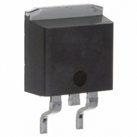
IRFS11N50APBF Vishay, IRFS11N50APBF Datasheet - Page 6

IRFS11N50APBF
Manufacturer Part Number
IRFS11N50APBF
Description
MOSFET N-CH 500V 11A D2PAK
Manufacturer
Vishay
Specifications of IRFS11N50APBF
Transistor Polarity
N-Channel
Fet Type
MOSFET N-Channel, Metal Oxide
Fet Feature
Standard
Rds On (max) @ Id, Vgs
520 mOhm @ 6.6A, 10V
Drain To Source Voltage (vdss)
500V
Current - Continuous Drain (id) @ 25° C
11A
Vgs(th) (max) @ Id
4V @ 250µA
Gate Charge (qg) @ Vgs
52nC @ 10V
Input Capacitance (ciss) @ Vds
1423pF @ 25V
Power - Max
170W
Mounting Type
Surface Mount
Package / Case
D²Pak, TO-263 (2 leads + tab)
Minimum Operating Temperature
- 55 C
Configuration
Single
Resistance Drain-source Rds (on)
0.52 Ohm @ 10 V
Drain-source Breakdown Voltage
500 V
Gate-source Breakdown Voltage
+/- 30 V
Continuous Drain Current
11 A
Power Dissipation
170000 mW
Maximum Operating Temperature
+ 150 C
Mounting Style
SMD/SMT
Continuous Drain Current Id
11A
Drain Source Voltage Vds
500V
On Resistance Rds(on)
520mohm
Rds(on) Test Voltage Vgs
10V
Threshold Voltage Vgs Typ
4V
Lead Free Status / RoHS Status
Lead free / RoHS Compliant
Lead Free Status / RoHS Status
Lead free / RoHS Compliant, Lead free / RoHS Compliant
Other names
*IRFS11N50APBF
Available stocks
Company
Part Number
Manufacturer
Quantity
Price
IRFS11N50A, SiHFS11N50A
Vishay Siliconix
www.vishay.com
6
Fig. 12c - Maximum Avalanche Energy vs. Drain Current
V
Fig. 13a - Basic Gate Charge Waveform
GS
V
G
Q
GS
Charge
Q
Q
GD
G
Fig. 12d - Typical Drain-to-Source Voltage
Fig. 13b - Gate Charge Test Circuit
12 V
V
GS
Same type as D.U.T.
Current regulator
vs. Avalanche Current
0.2 µF
Current sampling resistors
3 mA
50 kΩ
0.3 µF
I
G
S10-2326-Rev. B, 18-Oct-10
Document Number: 91286
D.U.T.
I
D
+
-
V
DS


