STD50N03L STMicroelectronics, STD50N03L Datasheet
STD50N03L
Specifications of STD50N03L
STD50N03L
Available stocks


Related parts for STD50N03L


STD50N03L Summary of contents
Page 1
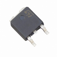
... October 2006 N-CHANNEL 30V - 9.2mΩ - 40A - DPAK/IPAK STripFET™ III Power MOSFET R I DS(on) D 10.5mΩ 40A 10.5mΩ 40A Internal schematic diagram Marking D50N03L D50N03L Rev 2 STD50N03L STD50N03L DPAK IPAK Package Packaging DPAK Tape & reel IPAK Tube 3 1 1/16 www ...
Page 2
... Contents Contents 1 Electrical ratings . . . . . . . . . . . . . . . . . . . . . . . . . . . . . . . . . . . . . . . . . . . . 3 2 Electrical characteristics . . . . . . . . . . . . . . . . . . . . . . . . . . . . . . . . . . . . . 4 2.1 Electrical characteristics (curves) 3 Test circuit 4 Package mechanical data . . . . . . . . . . . . . . . . . . . . . . . . . . . . . . . . . . . . 11 5 Packaging mechanical data . . . . . . . . . . . . . . . . . . . . . . . . . . . . . . . . . . 14 6 Revision history . . . . . . . . . . . . . . . . . . . . . . . . . . . . . . . . . . . . . . . . . . . 15 2/ STD50N03L - STD50N03L ...
Page 3
... STD50N03L - STD50N03L-1 1 Electrical ratings Table 1. Absolute maximum ratings Symbol V Drain-source voltage ( Gate-source voltage GS (1) I Drain current (continuous Drain current (continuous (2) I Drain current (pulsed Total dissipation at T TOT Derating factor (3) E Single pulse avalanche energy AS T Operating junction temperature J Storage temperature ...
Page 4
... Test conditions V =25V, f=1MHz 15V (see Figure 13 24V ; V DS f=1MHz Gate Bias Bias=0 Test signal Level=20mV open drain ; See Appendix A OSS gd gd STD50N03L - STD50N03L-1 Min. Typ 250µ 20A 9 20A 0.012 0.019 Min. Typ. Max. 1434 294 48 = 40A 10.4 D 5.1 3 ...
Page 5
... STD50N03L - STD50N03L-1 Table 5. Switching times Symbol t Turn-on delay time d(on) t Rise time r t Turn-off delay time d(off) t Fall time f Table 6. Source drain diode Symbol Source-drain current I SD Source-drain current (1) I SDM (pulsed) (2) Forward on voltage Reverse recovery time rr Q Reverse recovery charge ...
Page 6
... Electrical characteristics 2.1 Electrical characteristics (curves) Figure 1. Safe operating area Figure 3. Output characteristics Figure 5. Normalized B VDSS 6/16 Figure 2. Figure 4. vs temperature Figure 6. STD50N03L - STD50N03L-1 Thermal impedance Transfer characteristics Static drain-source on resistance ...
Page 7
... STD50N03L - STD50N03L-1 Figure 7. Gate charge vs gate-source voltage Figure 8. Figure 9. Normalized gate threshold voltage vs temperature Figure 11. Source-drain diode forward characteristics Electrical characteristics Capacitance variations Figure 10. Normalized on resistance vs temperature 7/16 ...
Page 8
... Figure 12. Switching times test circuit for resistive load Figure 14. Test circuit for inductive load switching and diode recovery times Figure 16. Unclamped inductive waveform 8/16 STD50N03L - STD50N03L-1 Figure 13. Gate charge test circuit Figure 15. Unclamped Inductive load test circuit Figure 17. Switching time waveform ...
Page 9
... STD50N03L - STD50N03L-1 Appendix A Buck converter Figure 18. Power losses estimation The power losses associated with the FETs in a Synchronous Buck converter can be estimated using the equations shown in the table below. The formulas give a good approximation, for the sake of performance comparison, of how different pairs of devices affect the converter efficiency ...
Page 10
... Not applicable g(SW1 oss(SW1) 2 Duty-cycle Post threshold gate charge Third quadrant gate charge On state losses On-off transition losses Conduction and reverse recovery diode losses Gate drive losses Output capacitance losses STD50N03L - STD50N03L-1 Low side switch (SW2 DS(on)SW2 L I Zero Voltage Switching rr(SW2 ...
Page 11
... STD50N03L - STD50N03L-1 4 Package mechanical data In order to meet environmental requirements, ST offers these devices in ECOPACK® packages. These packages have a Lead-free second level interconnect . The category of second level interconnect is marked on the package and on the inner box label, in compliance with JEDEC Standard JESD97. The maximum ratings related to soldering conditions are also marked on the inner box label ...
Page 12
... STD50N03L - STD50N03L-1 inch MIN. TYP. MAX. 0.086 0.094 0.035 0.043 0.027 0.051 0.025 0.031 0.204 0.212 0.033 0.012 0.037 0.017 0.023 0.019 0.023 0.236 0.244 ...
Page 13
... STD50N03L - STD50N03L-1 DIM (L1 DPAK MECHANICAL DATA mm. MIN. TYP MAX. 2.2 2.4 0.9 1.1 0.03 0.23 0.64 0.9 5.2 5.4 0.45 0.6 0.48 0.6 6 6.2 5.1 6.4 6.6 4.7 2.28 4.4 4.6 9.35 10.1 1 2.8 0.8 0.6 1 0.2 0° 8° Package mechanical data inch MIN ...
Page 14
... MIN. MAX. 0.267 0.275 0.409 0.417 0.476 0.059 0.063 0.059 0.065 0.073 0.291 0.299 0.100 0.108 0.153 0.161 0.311 0.319 0.075 0.082 1.574 0.618 0.641 STD50N03L - STD50N03L-1 REEL MECHANICAL DATA mm inch DIM. MIN. MAX. MIN. MAX. A 330 12.992 B 1.5 0.059 C 12.8 13 ...
Page 15
... STD50N03L - STD50N03L-1 6 Revision history Table 9. Revision history Date 31-Jul-2006 27-Oct-2006 Revision 1 Initial release. 2 Modified Figure 1.: Safe operating area on page 6 Revision history Changes 15/16 ...
Page 16
... Australia - Belgium - Brazil - Canada - China - Czech Republic - Finland - France - Germany - Hong Kong - India - Israel - Italy - Japan - Malaysia - Malta - Morocco - Singapore - Spain - Sweden - Switzerland - United Kingdom - United States of America 16/16 Please Read Carefully: © 2006 STMicroelectronics - All rights reserved STMicroelectronics group of companies www.st.com STD50N03L - STD50N03L-1 ...