BSP220,115 NXP Semiconductors, BSP220,115 Datasheet - Page 3
BSP220,115
Manufacturer Part Number
BSP220,115
Description
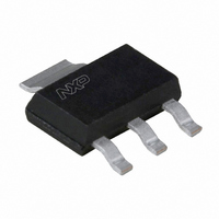
MOSFET P-CH 200V 225MA SOT223
Manufacturer
NXP Semiconductors
Datasheet
1.BSP220115.pdf
(12 pages)
Specifications of BSP220,115
Package / Case
SOT-223 (3 leads + Tab), SC-73, TO-261
Mounting Type
Surface Mount
Power - Max
1.5W
Fet Type
MOSFET P-Channel, Metal Oxide
Vgs(th) (max) @ Id
2.8V @ 1mA
Current - Continuous Drain (id) @ 25° C
225mA
Drain To Source Voltage (vdss)
200V
Fet Feature
Logic Level Gate
Rds On (max) @ Id, Vgs
12 Ohm @ 200mA, 10V
Minimum Operating Temperature
- 65 C
Configuration
Single Dual Drain
Transistor Polarity
P-Channel
Resistance Drain-source Rds (on)
12 Ohm @ 10 V
Drain-source Breakdown Voltage
200 V
Gate-source Breakdown Voltage
+/- 20 V
Continuous Drain Current
0.225 A
Power Dissipation
1500 mW
Maximum Operating Temperature
+ 150 C
Mounting Style
SMD/SMT
Lead Free Status / RoHS Status
Lead free / RoHS Compliant
Gate Charge (qg) @ Vgs
-
Lead Free Status / Rohs Status
Lead free / RoHS Compliant
Other names
934000490115::BSP220 T/R::BSP220 T/R


Philips Semiconductors
LIMITING VALUES
In accordance with the Absolute Maximum System (IEC 134).
Note
1. Device mounted on an epoxy printed-circuit board 40 x 40 x 1.5 mm; mounting pad for the drain lead minimum 6 cm
THERMAL RESISTANCE
Note
1. Device mounted on an epoxy printed-circuit board 40 x 40 x 1.5 mm; mounting pad for the drain lead minimum 6 cm
April 1995
P
T
T
R
SYMBOL
SYMBOL
V
V
I
I
stg
j
tot
th j-a
P-channel enhancement mode vertical
D-MOS transistor
D
DM
DS
GSO
drain-source voltage
gate-source voltage
drain current
drain current
total power dissipation
storage temperature range
junction temperature
from junction to ambient (note 1)
PARAMETER
PARAMETER
3
open drain
DC value
peak value
up to T
amb
CONDITIONS
= 25 C (note 1)
83.3
MIN.
65
VALUE
Product specification
200
20
225
600
1.5
150
150
BSP220
MAX.
K/W
UNIT
V
V
mA
mA
W
UNIT
C
C
2
2
.
.
Related parts for BSP220,115
Image
Part Number
Description
Manufacturer
Datasheet
Request
R

Part Number:
Description:
Intermediate level P-channel enhancement mode Field-Effect Transistor (FET) in a plastic package using vertical D-MOS technology
Manufacturer:
NXP Semiconductors
Datasheet:

Part Number:
Description:
NXP Semiconductors designed the LPC2420/2460 microcontroller around a 16-bit/32-bitARM7TDMI-S CPU core with real-time debug interfaces that include both JTAG andembedded trace
Manufacturer:
NXP Semiconductors
Datasheet:

Part Number:
Description:
NXP Semiconductors designed the LPC2458 microcontroller around a 16-bit/32-bitARM7TDMI-S CPU core with real-time debug interfaces that include both JTAG andembedded trace
Manufacturer:
NXP Semiconductors
Datasheet:
Part Number:
Description:
NXP Semiconductors designed the LPC2468 microcontroller around a 16-bit/32-bitARM7TDMI-S CPU core with real-time debug interfaces that include both JTAG andembedded trace
Manufacturer:
NXP Semiconductors
Datasheet:
Part Number:
Description:
NXP Semiconductors designed the LPC2470 microcontroller, powered by theARM7TDMI-S core, to be a highly integrated microcontroller for a wide range ofapplications that require advanced communications and high quality graphic displays
Manufacturer:
NXP Semiconductors
Datasheet:
Part Number:
Description:
NXP Semiconductors designed the LPC2478 microcontroller, powered by theARM7TDMI-S core, to be a highly integrated microcontroller for a wide range ofapplications that require advanced communications and high quality graphic displays
Manufacturer:
NXP Semiconductors
Datasheet:
Part Number:
Description:
The Philips Semiconductors XA (eXtended Architecture) family of 16-bit single-chip microcontrollers is powerful enough to easily handle the requirements of high performance embedded applications, yet inexpensive enough to compete in the market for hi
Manufacturer:
NXP Semiconductors
Datasheet:
Part Number:
Description:
The XA-S3 device is a member of Philips Semiconductors? XA(eXtended Architecture) family of high performance 16-bitsingle-chip microcontrollers
Manufacturer:
NXP Semiconductors
Datasheet:

Part Number:
Description:
The NXP BlueStreak LH75401/LH75411 family consists of two low-cost 16/32-bit System-on-Chip (SoC) devices
Manufacturer:
NXP Semiconductors
Datasheet:
Part Number:
Description:
The NXP LPC3130/3131 combine an 180 MHz ARM926EJ-S CPU core, high-speed USB2
Manufacturer:
NXP Semiconductors
Datasheet:
Part Number:
Description:
The NXP LPC3141 combine a 270 MHz ARM926EJ-S CPU core, High-speed USB 2
Manufacturer:
NXP Semiconductors
Part Number:
Description:
The NXP LPC3143 combine a 270 MHz ARM926EJ-S CPU core, High-speed USB 2
Manufacturer:
NXP Semiconductors

Part Number:
Description:
The NXP LPC3152 combines an 180 MHz ARM926EJ-S CPU core, High-speed USB 2
Manufacturer:
NXP Semiconductors
Part Number:
Description:
The NXP LPC3154 combines an 180 MHz ARM926EJ-S CPU core, High-speed USB 2
Manufacturer:
NXP Semiconductors