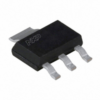
BSP250,115 NXP Semiconductors, BSP250,115 Datasheet - Page 3

BSP250,115
Manufacturer Part Number
BSP250,115
Description
MOSFET P-CH 30V 3A SOT223
Manufacturer
NXP Semiconductors
Datasheet
1.BSP250135.pdf
(12 pages)
Specifications of BSP250,115
Package / Case
SOT-223 (3 leads + Tab), SC-73, TO-261
Mounting Type
Surface Mount
Power - Max
1.65W
Fet Type
MOSFET P-Channel, Metal Oxide
Gate Charge (qg) @ Vgs
25nC @ 10V
Vgs(th) (max) @ Id
2.8V @ 1mA
Current - Continuous Drain (id) @ 25° C
3A
Drain To Source Voltage (vdss)
30V
Fet Feature
Logic Level Gate
Rds On (max) @ Id, Vgs
250 mOhm @ 1A, 10V
Minimum Operating Temperature
- 65 C
Configuration
Single Dual Drain
Transistor Polarity
P-Channel
Resistance Drain-source Rds (on)
0.25 Ohm @ 10 V
Gate Charge Qg
10 nC
Forward Transconductance Gfs (max / Min)
2 S, 1 S
Drain-source Breakdown Voltage
30 V
Gate-source Breakdown Voltage
+/- 20 V
Continuous Drain Current
3 A
Power Dissipation
1650 mW
Maximum Operating Temperature
+ 150 C
Mounting Style
SMD/SMT
Lead Free Status / RoHS Status
Lead free / RoHS Compliant
Lead Free Status / RoHS Status
Lead free / RoHS Compliant, Lead free / RoHS Compliant
Other names
934033450115::BSP250 T/R::BSP250 T/R
Available stocks
Company
Part Number
Manufacturer
Quantity
Price
Part Number:
BSP250,115
Manufacturer:
NEXPERIA/安世
Quantity:
20 000
Philips Semiconductors
LIMITING VALUES
In accordance with the Absolute Maximum Rating System (IEC 134).
Notes
1. Pulse width and duty cycle limited by maximum junction temperature.
2. Device mounted on an epoxy printed-circuit board, 40
1997 Jun 20
handbook, halfpage
V
V
I
I
P
T
T
Source-drain diode
I
I
SYMBOL
D
DM
S
SM
stg
j
DS
GSO
tot
P-channel enhancement mode
vertical D-MOS transistor
P tot
(W)
2.0
1.6
1.2
0.8
0.4
0
0
drain-source voltage (DC)
gate-source voltage (DC)
drain current (DC)
peak drain current
total power dissipation
storage temperature
operating junction temperature
source current (DC)
peak pulsed source current
Fig.2 Power derating curve.
50
100
PARAMETER
150
T amb ( C)
MLB885
200
3
40
open drain
T
note 1
T
T
T
note 1
s
s
amb
s
handbook, halfpage
= 100 C
Soldering point temperature T
(1) R
100 C
100 C
1.5 mm; mounting pad for drain lead minimum 6 cm
= 25 C; note 2
= 0.01.
CONDITIONS
(A)
10
10
I D
10
10
DSon
10
1
2
1
2
1
limitation.
P
t p
T
Fig.3 SOAR.
1
=
s
(1)
t p
T
t
= 100 C.
65
MIN.
DC
10
Product specification
5
1.65
+150
150
V DS (V)
3
1.5
30
20
12
6
MAX.
10 s
BSP250
1 ms
t p =
MLB835
10
V
V
A
A
W
W
A
A
2
C
C
UNIT
2
.


