IRFS3207 International Rectifier, IRFS3207 Datasheet - Page 2
IRFS3207
Manufacturer Part Number
IRFS3207
Description
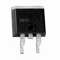
MOSFET N-CH 75V 180A D2PAK
Manufacturer
International Rectifier
Series
HEXFET®r
Datasheet
1.IRFB3207PBF.pdf
(12 pages)
Specifications of IRFS3207
Fet Type
MOSFET N-Channel, Metal Oxide
Fet Feature
Standard
Rds On (max) @ Id, Vgs
4.5 mOhm @ 75A, 10V
Drain To Source Voltage (vdss)
75V
Current - Continuous Drain (id) @ 25° C
180A
Vgs(th) (max) @ Id
4V @ 250µA
Gate Charge (qg) @ Vgs
260nC @ 10V
Input Capacitance (ciss) @ Vds
7600pF @ 50V
Power - Max
330W
Mounting Type
Surface Mount
Package / Case
D²Pak, TO-263 (2 leads + tab)
Lead Free Status / RoHS Status
Contains lead / RoHS non-compliant
Other names
*IRFS3207
Available stocks
Company
Part Number
Manufacturer
Quantity
Price
Company:

Part Number:
IRFS3207
Manufacturer:
IR
Quantity:
12 500
Part Number:
IRFS3207TRLPBF
Manufacturer:
IR
Quantity:
20 000
Part Number:
IRFS3207Z
Manufacturer:
IR
Quantity:
20 000
Company:
Part Number:
IRFS3207ZPBF
Manufacturer:
IR
Quantity:
12 500
Part Number:
IRFS3207ZPBF
Manufacturer:
IR
Quantity:
20 000


Notes:
‚
ƒ
„
…
V
∆V
R
V
I
I
R
gfs
Q
Q
Q
t
t
t
t
C
C
C
C
C
I
I
V
t
Q
I
t
Static @ T
Dynamic @ T
Diode Characteristics
DSS
GSS
d(on)
r
d(off)
f
S
SM
rr
RRM
on
(BR)DSS
DS(on)
GS(th)
G
iss
oss
rss
oss
oss
SD
g
gs
gd
rr
temperature. Package limitation current is 75A
above this value.
Calculated continuous current based on maximum allowable junction
Repetitive rating; pulse width limited by max. junction
temperature.
Limited by T
I
Pulse width ≤ 400µs; duty cycle ≤ 2%.
2
R
Symbol
Symbol
Symbol
SD
(BR)DSS
G
eff. (ER) Effective Output Capacitance (Energy Related) –––
eff. (TR) Effective Output Capacitance (Time Related)
≤ 75A, di/dt ≤ 500A/µs, V
= 25Ω, I
/∆T
J
AS
Jmax
J
Drain-to-Source Breakdown Voltage
Breakdown Voltage Temp. Coefficient
Static Drain-to-Source On-Resistance
Gate Threshold Voltage
Drain-to-Source Leakage Current
Gate-to-Source Forward Leakage
Gate-to-Source Reverse Leakage
Gate Input Resistance
Forward Transconductance
Total Gate Charge
Gate-to-Source Charge
Gate-to-Drain ("Miller") Charge
Turn-On Delay Time
Rise Time
Turn-Off Delay Time
Fall Time
Input Capacitance
Output Capacitance
Reverse Transfer Capacitance
Continuous Source Current
(Body Diode)
Pulsed Source Current
(Body Diode)
Diode Forward Voltage
Reverse Recovery Time
Reverse Recovery Charge
Reverse Recovery Current
Forward Turn-On Time
= 75A, V
= 25°C (unless otherwise specified)
, starting T
J
= 25°C (unless otherwise specified)
Parameter
GS
=10V. Part not recommended for use
J
= 25°C, L = 0.33mH
DD
Ãdi
≤ V
Parameter
Parameter
(BR)DSS
, T
J
≤ 175°C.
Intrinsic turn-on time is negligible (turn-on is dominated by LS+LD)
Min. Typ. Max. Units
Min. Typ. Max. Units
Min. Typ. Max. Units
––– 0.069 –––
150
–––
–––
–––
–––
–––
–––
–––
–––
–––
–––
–––
–––
–––
–––
–––
–––
–––
–––
–––
–––
–––
–––
–––
–––
–––
2.0
†
‡
ˆ
‰
75
mended footprint and soldering techniques refer to application note #AN-994.
C
When mounted on 1" square PCB (FR-4 or G-10 Material). For recom
C
as C
C
oss
θ
oss
oss
7600
1010
–––
–––
–––
–––
–––
–––
–––
180
120
710
390
920
––– 180
–––
–––
3.6
1.2
2.6
eff. (TR) is a fixed capacitance that gives the same charging time
oss
eff. (ER) is a fixed capacitance that gives the same energy as
while V
48
68
29
68
74
42
49
65
92
while V
-200
DS
–––
250
200
–––
–––
260
–––
–––
–––
–––
–––
–––
–––
–––
–––
–––
–––
720
140
–––
4.5
4.0
1.3
20
63
74
98
DS
is rising from 0 to 80% V
™
is rising from 0 to 80% V
V/°C
mΩ
µA
nA
nC
nC
pF
ns
ns
Ω
V
V
S
A
V
A
V
Reference to 25°C, I
V
V
V
V
V
V
f = 1MHz, open drain
V
I
V
V
V
I
R
V
V
V
ƒ = 1.0MHz
V
V
MOSFET symbol
showing the
integral reverse
p-n junction diode.
T
T
T
T
T
T
D
D
J
J
J
J
J
J
GS
GS
DS
DS
DS
GS
GS
DS
DS
GS
DD
GS
GS
DS
GS
GS
G
= 75A
= 75A
= 25°C, I
= 25°C
= 125°C
= 25°C
= 125°C
= 25°C
= 2.6Ω
= V
= 75V, V
= 75V, V
= 50V, I
= 60V
= 50V
= 0V, I
= 10V, I
= 20V
= -20V
= 10V
= 48V
= 10V
= 0V
= 0V, V
= 0V, V
GS
, I
D
g
g
DSS
D
DS
DS
S
D
D
= 250µA
GS
GS
= 75A, V
= 250µA
= 75A
= 75A
DSS
.
= 0V to 60V
= 0V to 60V
Conditions
Conditions
Conditions
= 0V
= 0V, T
.
V
I
di/dt = 100A/µs
F
R
= 75A
D
g
= 64V,
GS
= 1mA
J
= 125°C
= 0V
j
d
www.irf.com
, See Fig.11
, See Fig. 5
g
G
g
S
D
Related parts for IRFS3207
Image
Part Number
Description
Manufacturer
Datasheet
Request
R

Part Number:
Description:
SCHOTTKY RECTIFIER
Manufacturer:
International Rectifier Corp.
Datasheet:
Part Number:
Description:
SCHOTTKY RECTIFIER
Manufacturer:
International Rectifier Corp.
Datasheet:
Part Number:
Description:
SCHOTTKY RECTIFIER
Manufacturer:
International Rectifier Corp.
Datasheet:
Part Number:
Description:
SCHOTTKY RECTIFIER
Manufacturer:
International Rectifier Corp.
Datasheet:
Part Number:
Description:
SCHOTTKY RECTIFIER
Manufacturer:
International Rectifier Corp.
Datasheet:
Part Number:
Description:
SCHOTTKY RECTIFIER
Manufacturer:
International Rectifier Corp.
Datasheet:
Part Number:
Description:
SCHOTTKY RECTIFIER
Manufacturer:
International Rectifier Corp.
Datasheet:
Part Number:
Description:
SCHOTTKY RECTIFIER
Manufacturer:
International Rectifier Corp.
Datasheet:
Part Number:
Description:
SCHOTTKY RECTIFIER
Manufacturer:
International Rectifier Corp.
Datasheet:
Part Number:
Description:
SCHOTTKY RECTIFIER
Manufacturer:
International Rectifier Corp.
Datasheet:
Part Number:
Description:
SCHOTTKY RECTIFIER
Manufacturer:
International Rectifier Corp.
Datasheet:
Part Number:
Description:
SCHOTTKY RECTIFIER
Manufacturer:
International Rectifier Corp.
Datasheet:
Part Number:
Description:
SCHOTTKY RECTIFIER
Manufacturer:
International Rectifier Corp.
Datasheet:
Part Number:
Description:
SCHOTTKY RECTIFIER
Manufacturer:
International Rectifier Corp.
Datasheet:
Part Number:
Description:
SCHOTTKY RECTIFIER
Manufacturer:
International Rectifier Corp.
Datasheet: