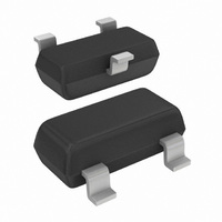
BSH103,215 NXP Semiconductors, BSH103,215 Datasheet - Page 2

BSH103,215
Manufacturer Part Number
BSH103,215
Description
MOSFET N-CH 30V 0.85A SOT23
Manufacturer
NXP Semiconductors
Datasheet
1.BSH103235.pdf
(12 pages)
Specifications of BSH103,215
Package / Case
SOT-23-3, TO-236-3, Micro3™, SSD3, SST3
Fet Type
MOSFET N-Channel, Metal Oxide
Fet Feature
Logic Level Gate
Rds On (max) @ Id, Vgs
400 mOhm @ 500mA, 4.5V
Drain To Source Voltage (vdss)
30V
Current - Continuous Drain (id) @ 25° C
850mA
Vgs(th) (max) @ Id
400mV @ 1mA
Gate Charge (qg) @ Vgs
2.1nC @ 4.5V
Input Capacitance (ciss) @ Vds
83pF @ 24V
Power - Max
540mW
Mounting Type
Surface Mount
Minimum Operating Temperature
- 55 C
Configuration
Single
Transistor Polarity
N-Channel
Resistance Drain-source Rds (on)
0.4 Ohm @ 4.5 V
Drain-source Breakdown Voltage
30 V
Gate-source Breakdown Voltage
+/- 8 V
Continuous Drain Current
0.85 A
Power Dissipation
500 mW
Maximum Operating Temperature
+ 150 C
Mounting Style
SMD/SMT
Lead Free Status / RoHS Status
Lead free / RoHS Compliant
Lead Free Status / RoHS Status
Lead free / RoHS Compliant, Lead free / RoHS Compliant
Other names
568-5013-2
934054713215
BSH103 T/R
BSH103 T/R
BSH103,215
934054713215
BSH103 T/R
BSH103 T/R
BSH103,215
Available stocks
Company
Part Number
Manufacturer
Quantity
Price
Company:
Part Number:
BSH103,215
Manufacturer:
TI
Quantity:
12 900
Part Number:
BSH103,215
Manufacturer:
NEXPERIA/安世
Quantity:
20 000
Philips Semiconductors
FEATURES
APPLICATIONS
DESCRIPTION
N-channel enhancement mode MOS transistor in a SOT23
SMD package.
QUICK REFERENCE DATA
1998 Feb 11
V
V
V
V
I
R
P
This product is supplied in anti-static packing to prevent damage caused by electrostatic discharge during transport
and handling. For further information, refer to Philips specs.: SNW-EQ-608, SNW-FQ-302A and SNW-FQ-302B.
D
Very low threshold
High-speed switching
No secondary breakdown
Direct interface to C-MOS, TTL etc.
Power management
DC to DC converters
Battery powered applications
‘Glue-logic’; interface between logic blocks and/or
periphery
General purpose switch.
DS
SD
GS
GSth
tot
DSon
N-channel enhancement mode
MOS transistor
SYMBOL
drain-source voltage (DC)
source-drain diode forward voltage
gate-source voltage (DC)
gate-source threshold voltage
drain current (DC)
drain-source on-state resistance
total power dissipation
PARAMETERS
CAUTION
V
V
T
V
T
2
s
s
GD
DS
GS
= 80 C
= 80 C
PINNING - SOT23
handbook, halfpage
= V
= 2.5 V; I
= 0; I
CONDITIONS
GS
PIN
Top view
S
1
2
3
; I
= 0.5 A
D
Fig.1 Simplified outline and symbol.
D
= 1 mA
1
= 0.5 A
SYMBOL
3
g
s
d
0.4
MIN.
2
gate
source
drain
MAM273
Product specification
30
1
0.85
0.5
0.5
8
DESCRIPTION
MAX.
g
BSH103
d
s
V
V
V
V
A
W
UNIT


